MF0032M-05AAXX 데이터 시트보기 (PDF) - Mitsumi
부품명
상세내역
제조사
MF0032M-05AAXX Datasheet PDF : 32 Pages
| |||
Preliminary
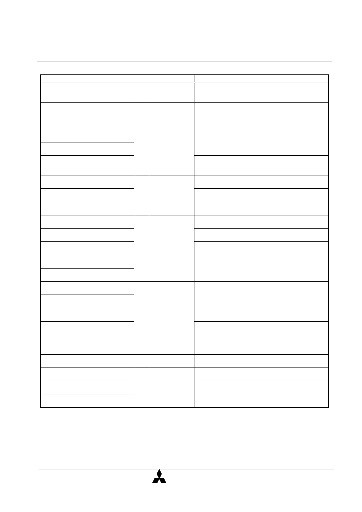
Signal Description
Signal Name
Address bus[A10-A0]
Data bus[D15-D0]
Card Enable[CE1#, CE2#]
(PC Card Memory Mode)
Card Enable[CE1#, CE2#]
(PC Card I/O Mode)
Chip Select[CS0#, CS1#]
(True IDE Interface)
Output Enable[OE#]
(PC Card Memory Mode)
Output Enable[OE#]
(PC Card I/O Mode)
ATA SEL#
(True IDE Interface)
Write Enable[WE#]
(PC Card Memory Mode)
Write Enable[WE#]
(PC Card I/O Mode)
Write Enable[WE#]
(True IDE Interface)
I/O Read[IORD#]
(PC Card I/O Mode)
I/O Read[IORD#]
(True IDE Interface)
I/O Write[IOWR#]
(PC Card I/O Mode)
I/O Write[IOWR#]
(True IDE Interface)
Ready[READY]
(PC Card Memory Mode)
IREQ#
(PC Card I/O Mode)
INTRQ
(True IDE Interface)
Card Detection[CD1#, CD2#]
Write Protect[WP]
(PC Card Memory Mode)
IOIS16#
(PC Card I/O Mode)
IOCS16#
(True IDE Interface)
MITSUBISHI STORAGE CARD
MF0XXXX-05AAXX series
CompactFlash CARDS
I/O
Pin No.
I 8, 10, 11, 12,
14, 15, 16, 17,
18, 19, 20
I/O 31, 30, 29, 28,
27, 49, 48, 47,
6, 5, 4, 3, 2,
23, 22, 21
I 7, 32
Description
Signals A10-A0 are address bus. A0 is invalid in
word mode. A10 is the MSB and A0 is the LSB.
Signals D15-D0 are data bus. D0 is the LSB of the
Even Byte of the Word. D8 is the LSB of the Odd
Byte of the Word.
CE1# and CE2# are low active card select signals.
I9
I 36
I 34
I 35
O 37
O 26, 25
O 24
In True IDE Interface, CS0# is used to select the
Command Block Registers. CS1# is used to select
the Control Block Registers.
OE# is used to gate Attribute and Common
Memory Read data from the Card.
OE# is used to gate Attribute Memory Read data
from the Card.
To enable True IDE Interface, this input should be
grounded by the host.
WE# is used for strobing Attribute and Common
Memory Write data into the Card.
WE# is used for strobing Attribute Memory Write
data into the Card.
This input should be connected Vcc by the host.
IORD# is used to read data from the Card’s I/O
space.
IOWR# is used to write data to the Card’s I/O
space.
READY signal is set high when the Card is ready to
accept a new data transfer operation.
This signal of low level is indicates that the card is
requesting software service to host, and high level
indicates that the card is not requesting.
This signal is active high interrupt request to the
host.
CD1# and CD2# provided for proper detection of
Card insertion.
This signal is held low because this card does not
have a write protect switch.
This output signal is asserted when the I/O port
address is capable of 16-bit access.
MITSUBISHI
ELECTRIC
3
June.2001. Rev. 1.3
Share Link: 