MF365A-LYCATXX 데이터 시트보기 (PDF) - Mitsumi
부품명
상세내역
제조사
MF365A-LYCATXX Datasheet PDF : 14 Pages
| |||
MITSUBISHI MEMORY CARD
STATIC RAM CARDS
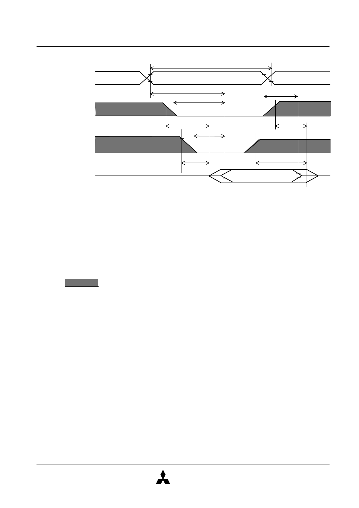
TIMING DIAGRAM (Attribute)
Read Cycle
VIH
An
VIL
VIH
CE#
VIL
VIH
OE#
VIL
VOH
Dm
(DOUT) VOL
Hi-Z
tcRR
ta(A)R
ta(CE)R
tV(A)R
ten(CE)R
ta(OE)R
tdis(CE)R
ten(OE)R
tdis(OE)R
OUTPUT VALID
WE#=“H” level
REG#=“L” level
Note 5 : Test Conditions
Input pulse levels
: VIL=0.4V, VIH=4.0V
Input pulse rise, fall time : tr=tf=10ns
Reference voltage
Input
: VIL=0.8V, VIH=3.5V
Output
: VOL=0.8V, VOH=3.0V
(ten and tdis are measured when output voltage is ± 500mV from steady state. )
Load
: 100pF + 1 TTL gate
5pF + 1 TTL gate (at ten and tdis measuring)
6:
Indicates the don’t care input
7 : Writing is executed in overlap of CE# and WE# are “L” level. (only for Common Memory)
8 : Don’t apply inverted phase signal externally when Dm pin is in output mode.
9 : CE# is indicated as follows:
Read A/Write A : CE#=CE1#=CE2#
Read B/Write B : CE#=CE1#, CE2#=“H” level
Read C/Write C : CE#=CE2#, CE1#=“H” level
MITSUBISHI
ELECTRIC
10/14
Apr. 1999 Rev. 1.2
Share Link: 