MJD243T4 데이터 시트보기 (PDF) - Motorola => Freescale
부품명
상세내역
제조사
MJD243T4 Datasheet PDF : 6 Pages
| |||
ÎÎÎÎÎÎÎÎÎÎÎÎÎÎÎÎÎÎÎÎÎÎÎÎÎÎÎÎÎÎÎÎÎÎÎÎÎÎÎÎÎÎÎÎÎÎÎÎÎÎÎÎÎÎÎÎÎÎÎÎÎÎÎÎÎÎÎÎ MJD243
ÎÎÎÎÎÎÎÎÎÎÎÎÎÎÎÎÎÎÎÎÎÎÎÎÎÎÎÎÎÎÎÎÎÎ ELECTRICAL CHARACTERISTICS (TC = 25_C unless otherwise noted)
ÎÎÎÎÎÎÎÎÎÎÎÎÎÎÎÎÎÎÎÎÎÎÎÎÎÎÎÎÎÎÎÎÎÎ Characteristic
Symbol
Min
ÎÎÎÎÎÎÎÎÎÎÎÎÎÎÎÎÎÎÎÎÎÎÎÎÎÎÎÎÎÎÎÎÎÎ OFF CHARACTERISTICS
ÎÎÎÎÎÎÎÎÎÎÎÎÎÎÎÎÎÎÎÎÎÎÎÎÎÎÎÎÎÎÎÎÎÎ Collector–Emitter Sustaining Voltage (1) (IC = 10 mAdc, IB = 0)
ÎÎÎÎÎÎÎÎÎÎÎÎÎÎÎÎÎÎÎÎÎÎÎÎÎÎÎÎÎÎÎÎÎÎ Collector Cutoff Current (VCB = 100 Vdc, IE = 0)
ÎÎÎÎÎÎÎÎÎÎÎÎÎÎÎÎÎÎÎÎÎÎÎÎÎÎÎÎÎÎÎÎÎÎ Collector Cutoff Current (VCB = 100 Vdc, IE = 0, TJ = 125_C)
VCEO(sus)
100
ICBO
—
—
ÎÎÎÎÎÎÎÎÎÎÎÎÎÎÎÎÎÎÎÎÎÎÎÎÎÎÎÎÎÎÎÎÎÎ Emitter Cutoff Current (VBE = 7 Vdc, IC = 0)
ÎÎÎÎÎÎÎÎÎÎÎÎÎÎÎÎÎÎÎÎÎÎÎÎÎÎÎÎÎÎÎÎÎÎ DC Current Gain (1) (IC = 200 mAdc, VCE = 1 Vdc)
ÎÎÎÎÎÎÎÎÎÎÎÎÎÎÎÎÎÎÎÎÎÎÎÎÎÎÎÎÎÎÎÎÎÎ DC Current Gain (1) (IC = 1 Adc, VCE = 1 Vdc)
IEBO
—
hFE
40
15
ÎÎÎÎÎÎÎÎÎÎÎÎÎÎÎÎÎÎÎÎÎÎÎÎÎÎÎÎÎÎÎÎÎÎ Collector–Emitter Saturation Voltage (1)
ÎÎÎÎÎÎÎÎÎÎÎÎÎÎÎÎÎÎÎÎÎÎÎÎÎÎÎÎÎÎÎÎÎÎ (IC = 500 mAdc, IB = 50 mAdc)
(IC = 1 Adc, IB = 100 mAdc)
VCE(sat)
—
—
ÎÎÎÎÎÎÎÎÎÎÎÎÎÎÎÎÎÎÎÎÎÎÎÎÎÎÎÎÎÎÎÎÎÎ Base–Emitter Saturation Voltage (1) (IC = 2 Adc, IB = 200 mAdc)
VBE(sat)
—
ÎÎÎÎÎÎÎÎÎÎÎÎÎÎÎÎÎÎÎÎÎÎÎÎÎÎÎÎÎÎÎÎÎÎ Base–Emitter On Voltage (1) (IC = 500 mAdc, VCE = 1 Vdc)
VBE(on)
—
ÎÎÎÎÎÎÎÎÎÎÎÎÎÎÎÎÎÎÎÎÎÎÎÎÎÎÎÎÎÎÎÎÎÎ DYNAMIC CHARACTERISTICS
ÎÎÎÎÎÎÎÎÎÎÎÎÎÎÎÎÎÎÎÎÎÎÎÎÎÎÎÎÎÎÎÎÎÎ Current–Gain — Bandwidth Product (2) (IC = 100 mAdc, VCE = 10 Vdc, ftest = 10 MHz)
fT
40
ÎÎÎÎÎÎÎÎÎÎÎÎÎÎÎÎÎÎÎÎÎÎÎÎÎÎÎÎÎÎÎÎÎÎÎÎÎÎÎÎÎÎÎÎÎÎÎÎÎÎÎÎÎÎÎÎÎÎÎÎÎÎÎÎÎÎÎÎ Output Capacitance (VCB = 10 Vdc, IE = 0, f = 0.1 MHz)
ÎÎÎÎÎÎÎÎÎÎÎÎÎÎÎÎÎÎÎÎÎÎÎÎÎÎÎÎÎÎÎÎÎÎ [ (1) Pulse Test: Pulse Width = 300 µs, Duty Cycle 2%.
Cob
—
Max
Unit
—
Vdc
100
nAdc
100
µAdc
100
nAdc
180
—
—
Vdc
0.3
0.6
1.8
Vdc
1.5
Vdc
—
MHz
50
pF
(2) fT = hFE• ftest.
10
5
2
1
0.5
0.2
0.1
0.05
0.02
0.01
1
500 µs
100 µs
1 ms
5 ms
dc
BONDING WIRE LIMITED
THERMALLY LIMITED @ TC = 25°C
(SINGLE PULSE)
SECOND BREAKDOWN LIMITED
CURVES APPLY BELOW
RATED VCEO
2
5
10
20
50 100
VCE, COLLECTOR–EMITTER VOLTAGE (VOLTS)
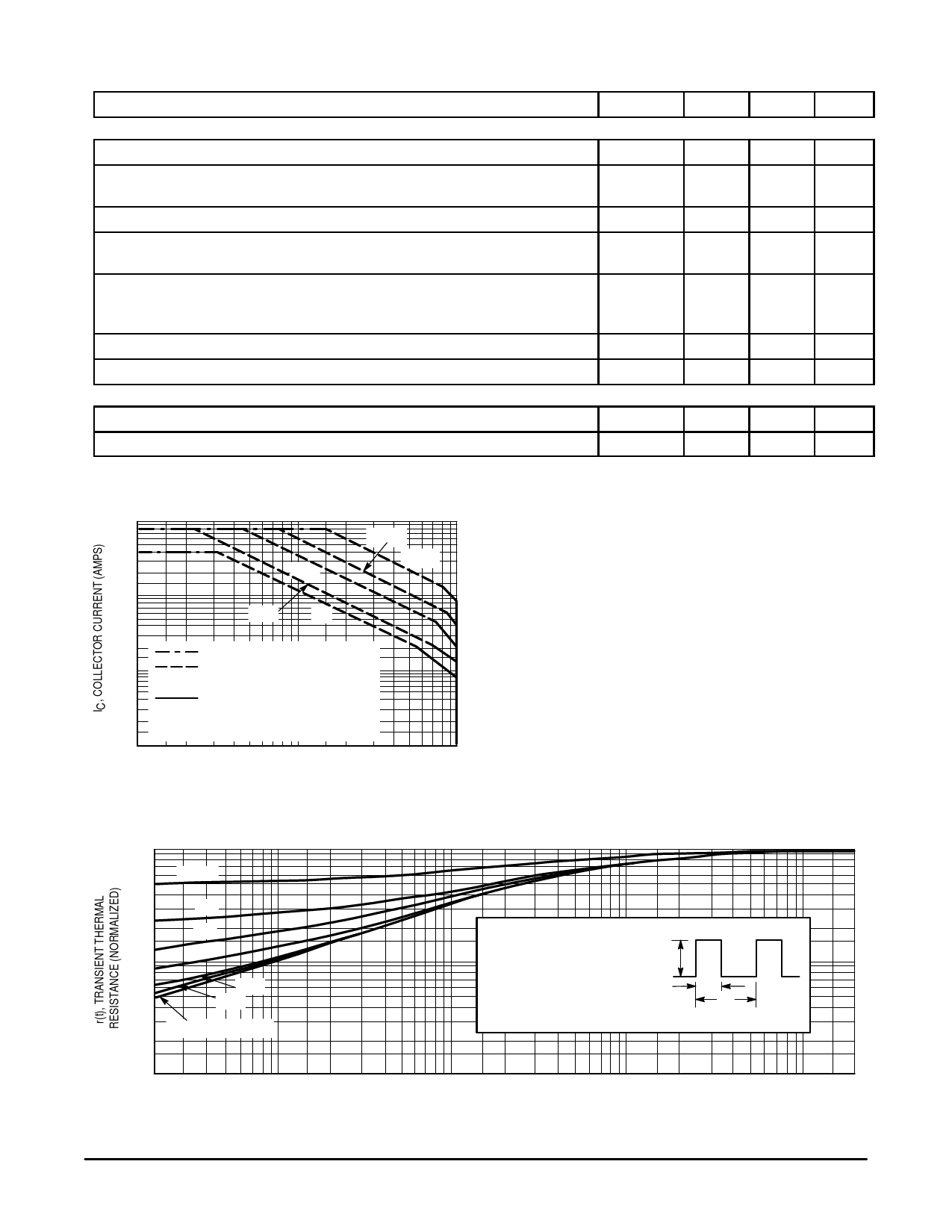
Figure 2. Active Region Maximum Safe
Operating Area
There are two limitations on the power handling ability of a
transistor: average junction temperature and second break-
down. Safe operating area curves indicate IC – VCE limits of
the transistor that must be observed for reliable operation;
i.e., the transistor must not be subjected to greater dissipa-
tion than the curves indicate.
The data of Figure 2 is based on TJ(pk) = 150_C; TC is
variable depending on conditions. Second breakdown pulse
vlimits are valid for duty cycles to 10% provided TJ(pk)
150_C. TJ(pk) may be calculated from the data in Fig-
ure 3. At high case temperatures, thermal limitations will re-
duce the power that can be handled to values less than the
limitations imposed by second breakdown.
1
0.7
0.5
D = 0.5
0.3
0.2
0.2
0.1
0.05
0.1
0.07
0.05
0.02
0.01
0.03
0 (SINGLE PULSE)
0.02
RθJC(t) = r(t) θJC
RθJC = 10°C/W MAX
D CURVES APPLY FOR POWER
PULSE TRAIN SHOWN
READ TIME AT t1
TJ(pk) – TC = P(pk) θJC(t)
P(pk)
t1
t2
DUTY CYCLE, D = t1/t2
0.01
0.02
0.05
0.1
0.2
0.5
1
2
5
10
20
t, TIME (ms)
Figure 3. Thermal Response
50
100
200
2
Motorola Bipolar Power Transistor Device Data
Share Link: 