ML7020 데이터 시트보기 (PDF) - Oki Electric Industry
부품명
상세내역
제조사
ML7020 Datasheet PDF : 19 Pages
| |||
1Semiconductor
FEDL7020-02
ML7020
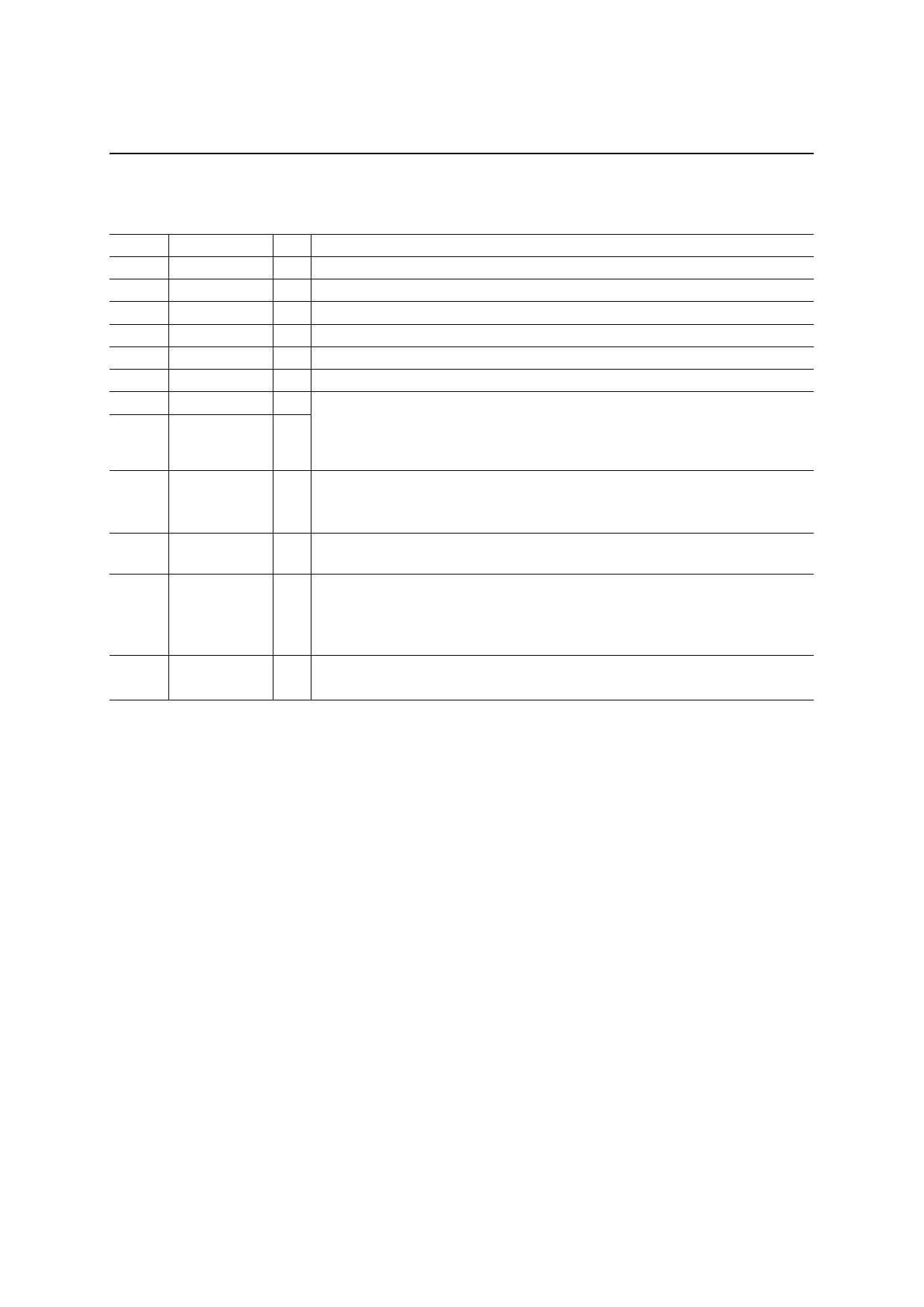
Pin No.
21
22
23
24
25
26
27
28
29
30
31
32
Symbol
A1
D0
D1
D2
D3
CLKOUT
X2
X1
XD
RD
DETB
SP
I/O
Description
I The address input pin A1 for the processor interface.
IO The data input/output pin D0 for the processor interface.
IO The data input/output pin D1 for the processor interface.
IO The data input/output pin D2 for the processor interface.
IO The data input/output pin D3 for the processor interface.
O The 3.579545 MHz oscillator circuit output pin.
O The pins for connecting a 3.579545 MHz crystal. The capacitors and the
feedback resistor are internally connected to these pins. When inputting an
I external clock, connect the input to the X1 pin via a 1000 pF capacitor and leave
the pin X2 open.
The modem transmit data input pin.
I The “1” level corresponds to the mark data and the “0” level corresponds to the
space data.
The modem receive data output pin. The mark and space data are the same as
O for XD. A mark is output when no carrier is detected.
The pin for outputting the carrier detect signal of the modem or the call progress
tone detector output.
O
The detection result corresponding to the respective operating mode is output
from this pin. A “0” indicates detection and a “1” indicates non-detection.
The DTMF reception detection output pin.
O
A “0” indicates detection and a “1” indicates non-detection.
5/19
Share Link: 