MM1381 데이터 시트보기 (PDF) - Mitsumi
부품명
상세내역
제조사
MM1381 Datasheet PDF : 10 Pages
| |||
MITSUMI
RGB Video Amplifier with OSD Input MM1381, 1382, 1383
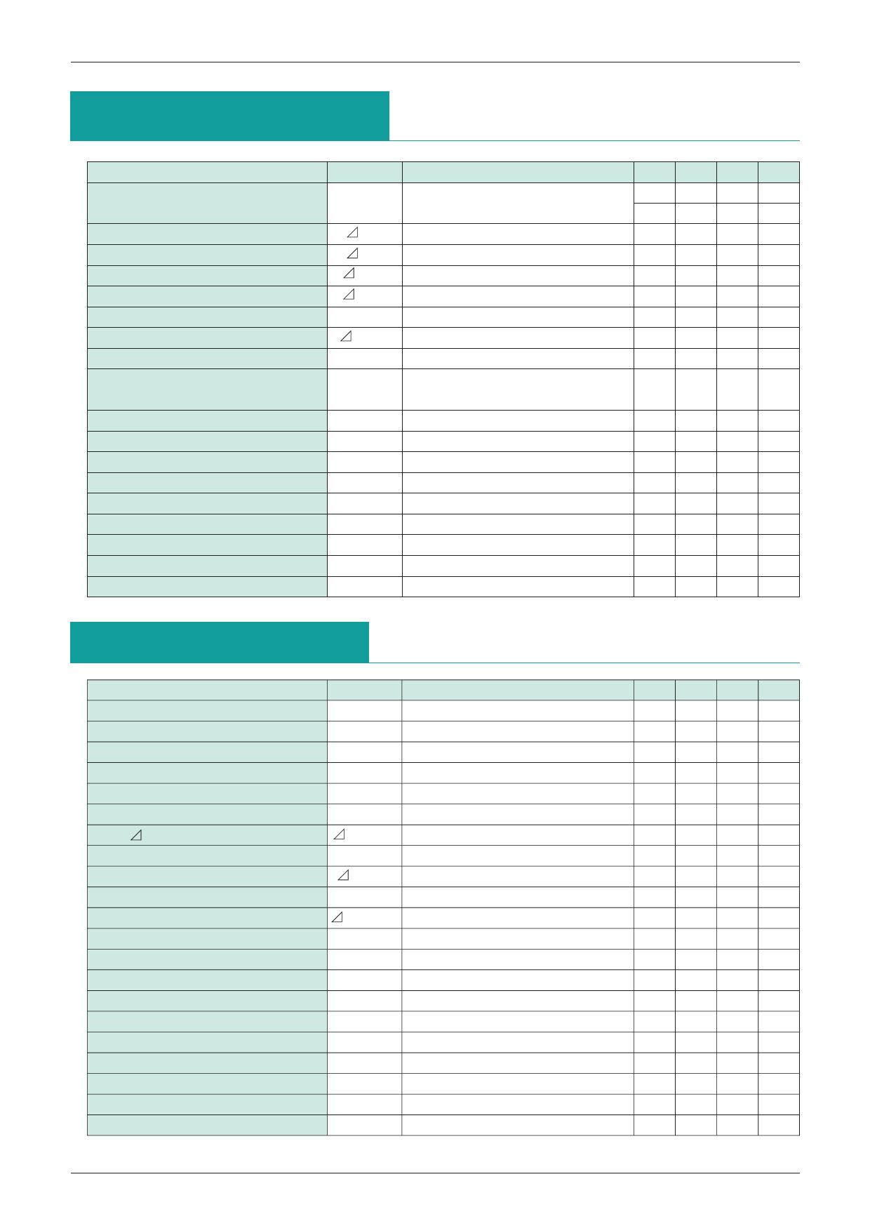
* AC Electrical Characteristics 14 (Except where noted otherwise, Ta=25°C, VCC1=VCC2=12V, V13=4V, V14=4V, VDRV=4V,
VCG=0V, VBG=4V, V4=0V. For AC tests, adjust output pins 16, 20 and 23 to 4V by hand.)
Item
Symbol
Video amp gain
AV max.
Contrast attenuation 1
Contrast attenuation 2
Drive attenuation 1
Drive attenuation 2
Gain matching
Gain change between amps
Video amp distortion
AV1
AV2
AVD1
AVD2
AVMAT
AVMAT
THD
Video amp frequency bandwidth
fBW
Video output rise time
Video output fall time
Video amp isolation 1
Video amp isolation 2
Blanking output rise time
Blanking output fall time
Blanking rise delay time
Blanking fall delay time
Back-porch clamping pulse width
tr
tf
VSEP1
VSEP2
tr-BLK
tf-BLK
trD-BLK
tfD-BLK
tpw
Measurement conditions
V13=4V, VDRV=4V
VIN=400mVP-P
V13=2V
V13=0.25V
VDRV=2V
VDRV=0.25V
* V13=VDRV=4V 8
* V13=4V~2V 9
VO=1VP-P, f=10kHz
V13=4V, VDRV=3V
* VO=4VP-P 10, 11
* VO=4VP-P 10
* VO=4VP-P 10
* V13=4V 12
* V13=4V 10, 12
* VO=1VP-P 10
* VO=1VP-P 10
VO=1VP-P
VO=1VP-P
*13
Min. Typ. Max. Units
7.5 10.0
V/V
16.9 20.0
dB
-6
dB
-40
dB
-4.5
dB
-11
dB
±0.3
dB
±0.2
dB
1
%
110
MHz
3.0
nS
4.0
nS
-70
dB
-50
dB
8
nS
14
nS
23
nS
20
nS
200
nS
OSD Electrical Characteristics
(Except where noted otherwise, Ta = 25°C, VCC1=VCC2=12V,
V13=4V, V14=4V, VDRV=4V, VCG=4V, VBG=4V, V4=4V, VC-o=1V)
Item
Input voltage OSD L
Input voltage OSD H
OSD selection input voltage L
OSD selection input voltage H
OSD selection input current L
OSD selection input current H
OSD black level output voltage
OSD output voltage VP-P
OSD output VP-P attenuation
Output adjustment between channels
Output fluctuation between channels
Video to OSD switching time
OSD-to-video switching time
Video to OSD transfer delay
OSD-to-video transport delay
OSD rise time
OSD fall time
OSD rise delay time
OSD fall delay time
Video isolation rate to OSD1
Video isolation rate to OSD2
Symbol
VOSDL
VOSDH
V4L
V4H
I4L
I4H
VOUT-OSD
VOSD-O
VOSD-O
VOSD-OMAT
VOSD-OMAT
tr-OSDSW
tr-OSDSW
trD-OSDSW
tfD-OSDSW
tr-OSD
tf-OSD
trD-OSD
tfD-OSD
Vfeed1
Vfeed2
Measurement conditions
V4=0V
V4=12V
VC-O=1V
V14=4V, VDRV=2V
V14=2V, VDRV=2V
V14=4V, VDRV=2V
V14=4V~2V, VDRV=2V
* V1=V2=V3=4V 15
* V1=V2=V3=4V 15
V1=V2=V3=V13=V14=4V
V1=V2=V3=V13=V14=4V
V14=4V
V14=4V
V14=4V
V14=4V
V14=4V, V1=V2=V3=0V
V14=4V, V1=V2=V3=0V
Min.
0.4
0.8
Typ.
1.2
1.6
1.2
1.6
-3.0
0.01
±85
4.5
50
±2.0
±3.5
4
11
11
12
4
10
6.5
9
-70
-60
Max. Units
V
2.0 V
V
2.0 V
-5.0 uA
2.0 uA
±175 mV
VP-P
30 %
%
%
nS
nS
nS
nS
nS
nS
nS
nS
dB
dB
Share Link: 