MSG33002 데이터 시트보기 (PDF) - Panasonic Corporation
부품명
상세내역
제조사
MSG33002 Datasheet PDF : 4 Pages
| |||
Transistors
MSG33002
SiGe HBT type
For low-noise RF amplifier
■ Features
• Compatible between high breakdown voltage and high cutoff fre-
quency
• Low-noise, high-gain amplification
• Suitable for high-density mounting and downsizing of the equip-
ment for Ultraminiature package
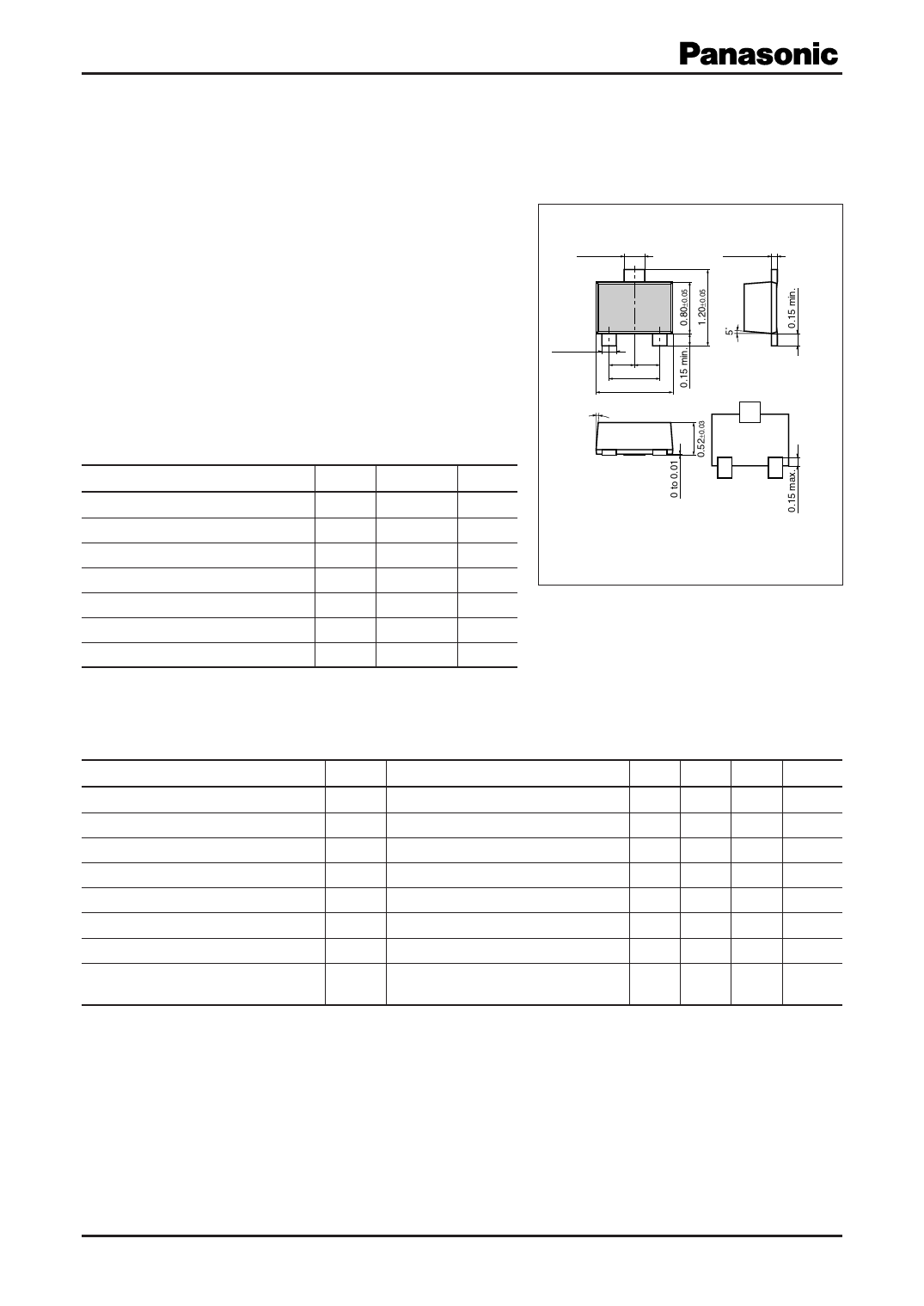
0.8 mm × 1.2 mm (height 0.52 mm)
0.33+–00..0025
3
0.23+–00..0025
12
(0.40) (0.40)
0.80±0.05
1.20±0.05
5˚
0.10+–00..0025
Unit: mm
■ Absolute Maximum Ratings Ta = 25°C
Parameter
Symbol Rating
Unit
Collector-base voltage (Emitter open) VCBO
9
V
Collector-emitter voltage (Base open) VCEO
6
V
Emitter-base voltage (Collector open) VEBO
1
V
Collector current
IC
60
mA
Collector power dissipation*
PC
100
mW
Junction temperature
Tj
125
°C
Storage temperature
Tstg −55 to +125 °C
Note) *: Copper plate at the collector is 5.0 cm2 on substrate at 10 mm × 12
mm × 0.8 mm.
Marking Symbol: 5T
1: Base
2: Emitter
3: Collector
SSSMini3-F1 Package
■ Electrical Characteristics Ta = 25°C ± 3°C
Parameter
Symbol
Conditions
Collector-base cutoff current (Emitter open)
Collector-emitter cutoff current (Base open)
Emitter-base cutoff current (Collector open)
Forward current transfer ratio
Transition frequency
Forward transfer gain
Noise figure
Collector output capacitance
(Common base, input open circuited)
ICBO
ICEO
IEBO
hFE
fT
S21e2
NF
Cob
VCB = 9 V, IE = 0
VCE = 6 V, IB = 0
VEB = 1 V, IC = 0
VCE = 3 V, IC = 6 mA
VCE = 3 V, IC = 20 mA, f = 2 GHz
VCE = 3 V, IC = 20 mA, f = 2 GHz
VCE = 3 V, IC = 6 mA, f = 2 GHz
VCB = 3 V, IE = 0, f = 1 MHz
Min Typ Max Unit
1
µA
1
µA
1
µA
100
220
19
GHz
7.5 10.5
dB
1.4 2.0
dB
0.4 0.7
pF
Note) Measuring methods are based on JAPANESE INDUSTRIAL STANDARD JIS C 7030 measuring methods for transistors.
Publication date: October 2004
SJC00293BED
1
Share Link: 