MSM6562B 데이터 시트보기 (PDF) - Oki Electric Industry
부품명
상세내역
제조사
MSM6562B Datasheet PDF : 50 Pages
| |||
¡ Semiconductor
MSM6562B-xx
(Note 1) Applies to the voltage drop (VC) from VDD, V1, V4 and V5 to each COMMON pin
(COM1 to COM16) as well as to voltage drop (VS) from VDD, V2, V3 and V5 to each
SEG pin (SEG1 to SEG100) when 40mA is flowed through one COM or SEG pin.
When output level is at VDD, V1, or V2 level, 40mA is flowed out, while 40mA is
flowed in when the output level is at V3, V4 or V5 level.
This occurs when 5V is input to VDD, V1 and V2 , and 0V is input to V3, V4 and
V5.
(Note 2) Applies to the current value flowed in the pin VDD, in the case of VDD = 5V,
VSS = 0V, V1, V2 = 5V, V3, V4, V5 = 0V and V5' is open.
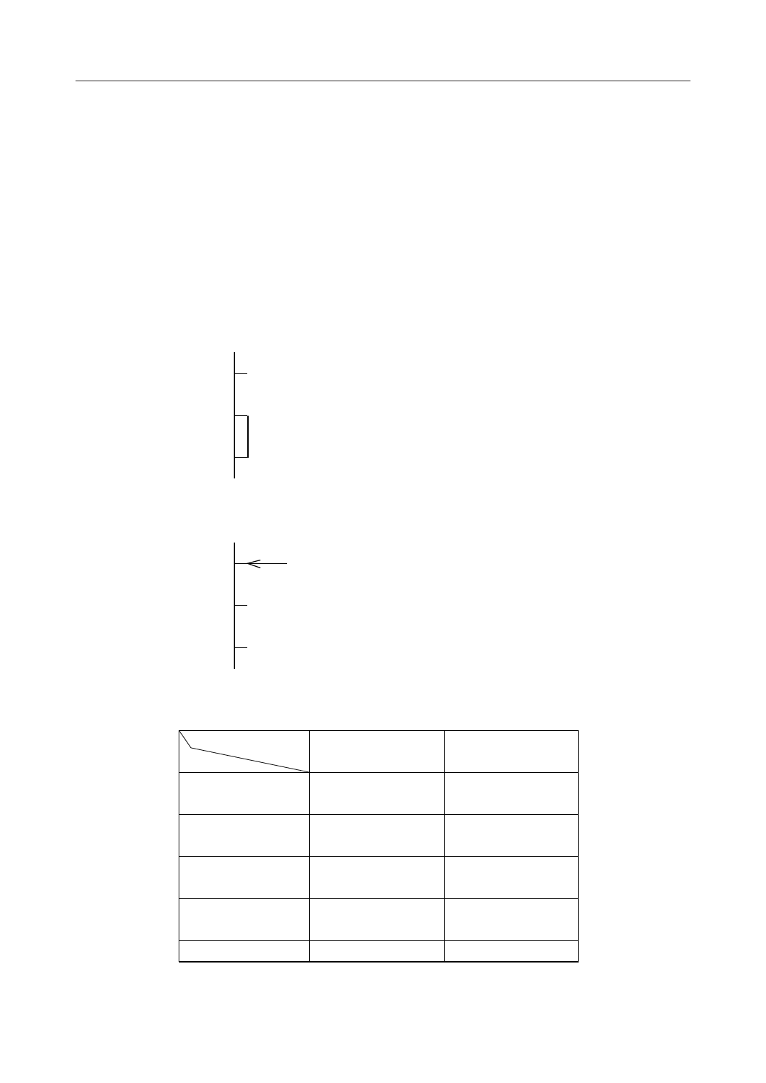
(Note 3) Built-in Rf oscillation circuit
OSC1
OSCR
Minimum wiring is required between OSCR and OSC2.
Leave OSC1 open.
OSC2
(Note
4) External clock input circuit
OSC1
Input pulse
Leave OSCR and OSC2 open.
OSCR
OSC2
(Note 5) Input the voltage to V5. (However, V5 cannot be used under VSS voltage.)
N (number of LCD lines)
Pin
V1
V2
V3
V4
V5
1-line mode
Bias : 1/4
VDD
–
VLCD
4
VDD
–
VLCD
2
VDD
–
VLCD
2
VDD
–
3VLCD
4
VDD – VLCD
2-line mode
Bias : 1/5
VDD
–
VLCD
5
VDD
–
2VLCD
5
VDD
–
3VLCD
5
VDD
–
4VLCD
5
VDD – VLCD
At 1/4 bias : Connect V2 and V3 externally and leave V3' open.
At 1/5 bias : Connect V3 and V3' externally.
VLCD is the LCD driving voltage. (For N [number of LCD lines], refer to
the explanation of the Function setting instruction of the instruction code.)
7/50
Share Link: 