MSM7717-02GS-K 데이터 시트보기 (PDF) - Oki Electric Industry
부품명
상세내역
제조사
MSM7717-02GS-K Datasheet PDF : 19 Pages
| |||
¡ Semiconductor
MSM7717-01/02/03
DG
Ground for the digital signal circuits.
This ground is separate from the analog signal ground AG. The DG pin must be connected to the
AG pin on the printed circuit board to make a common analog ground AG.
PDN
Power down control signal.
A logic "0" level drives both transmit and receive circuits to a power down state.
PCMOUT
PCM signal output.
Synchronizing with the rising edge of the BCLK signal, the PCM output signal is output from
MSD in a sequential order.
MSD may be output at the rising edge of the XSYNC signal, based on the timing between BCLK
and XSYNC.
This pin is in a high impedance state except during 8-bit PCM output. It is also in a high
impedance state during power saving or power down mode.
A pull-up resistor must be connected to this pin because its output is configured as an open drain.
This device is compatible with the ITU-T recommendation on coding law and output coding
format.
The MSM7717-03 (A-law) outputs the character signal, inverting the even bits.
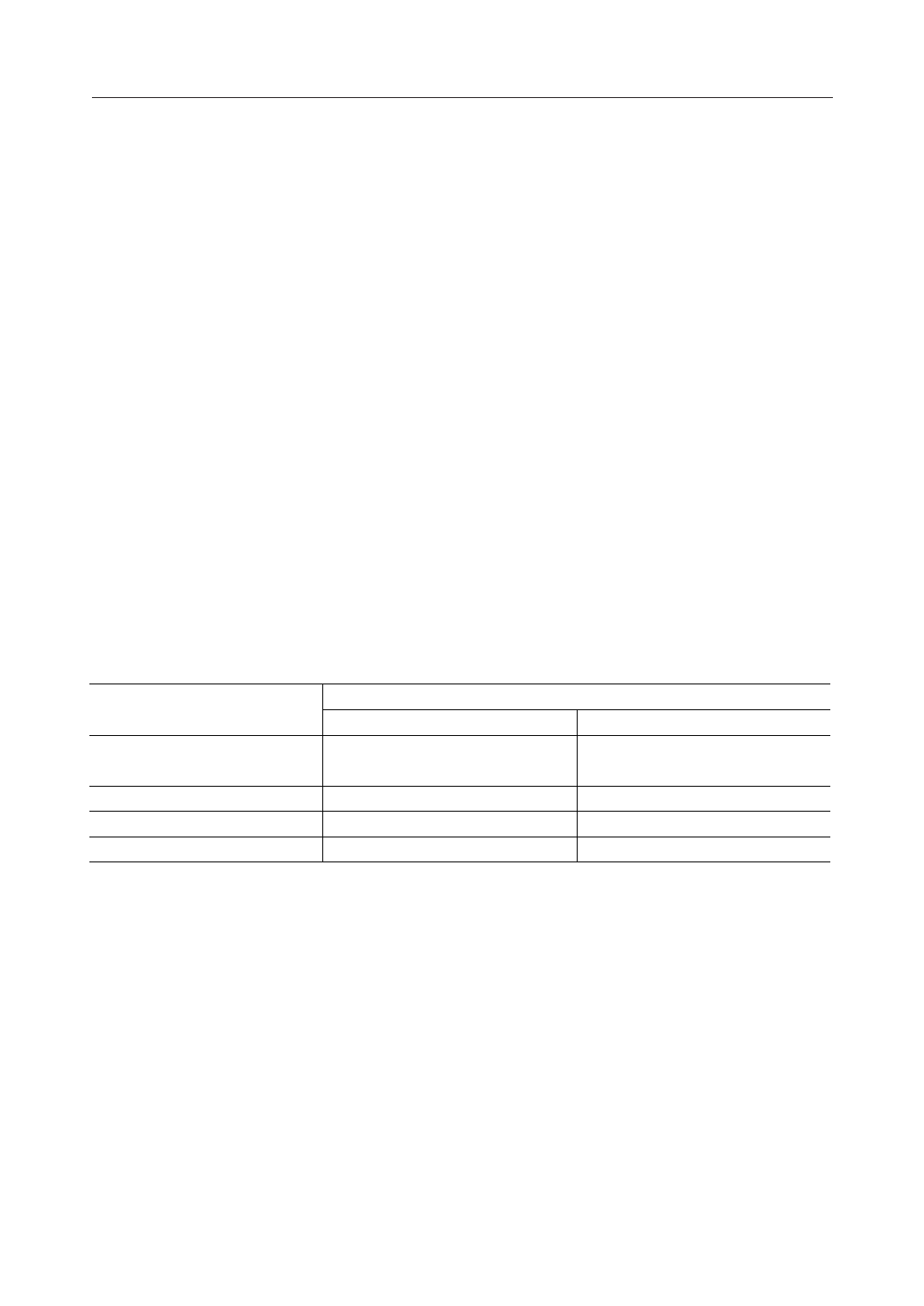
Input/Output Level
+Full scale
+0
–0
–Full scale
PCMIN/PCMOUT
MSM7717-02 (m-law)
MSM7717-03 (A-law)
MSD
MSD
1000 0000
1010 1010
1111 1111
1101 0101
0111 1111
0101 0101
0000 0000
0010 1010
7/19
Share Link: 