MT8812 데이터 시트보기 (PDF) - Mitel Networks
부품명
상세내역
제조사
MT8812 Datasheet PDF : 6 Pages
| |||
ISO-CMOS MT8812
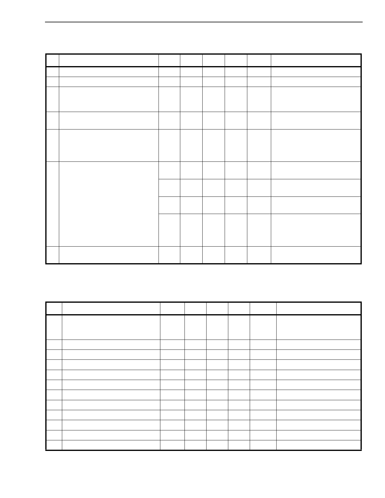
AC Electrical Characteristics† - Crosspoint Performance-VDC is the external DC offset applied at the analog
I/O pins. Voltages are with respect to VDD=7V, VDC=0V, VSS=-7V, unless otherwise stated.
Characteristics
Sym Min Typ‡ Max Units
Test Conditions
1 Switch I/O Capacitance
2 Feedthrough Capacitance
3 Frequency Response
Channel “ON”
20LOG(VOUT/VXi)=-3dB
4 Total Harmonic Distortion
(See G.5, G.6 in Appendix)
5 Feedthrough
Channel “OFF”
Feed.=20LOG (VOUT/VXi)
(See G.8 in Appendix)
CS
CF
F3dB
THD
FDT
20
0.2
45
0.01
-95
pF
pF
MHz
%
dB
f=1 MHz
f=1 MHz
Switch is “ON”; VINA = 2Vpp
sinewave; RL = 1kΩ
See Appendix, Fig. A.3
Switch is “ON”; VINA = 2Vpp
sinewave f= 1kHz; RL=1kΩ
All Switches “OFF”; VINA=
2Vpp sinewave f= 1kHz;
RL= 1kΩ.
See Appendix, Fig. A.4
6 Crosstalk between any two
Xtalk
-45
channels for switches Xi-Yi and
Xj-Yj.
-90
Xtalk=20LOG (VYj/VXi).
-85
(See G.7 in Appendix).
-80
dB VINA=2Vpp sinewave
f= 10MHz; RL = 75Ω.
dB VINA=2Vpp sinewave
f= 10kHz; RL = 600Ω.
dB VINA=2Vpp sinewave
f= 10kHz; RL = 1kΩ.
dB VINA=2Vpp sinewave
f= 1kHz; RL = 10kΩ.
Refer to Appendix, Fig. A.5
for test circuit.
7 Propagation delay through
tPS
switch
30
ns RL=1kΩ; CL=50pF
† Timing is over recommended temperature range. See Fig. 3 for control and I/O timing details.
‡ Typical figures are at 25°C and are for design aid only; not guaranteed and not subject to production testing.
Crosstalk measurements are for Plastic DIPS only, crosstalk values for PLCC packages are approximately 5dB better.
AC Electrical Characteristics† - Control and I/O Timings- VDC is the external DC offset applied at the analog
I/O pins. Voltages are with respect to VDD=7V, VDC=0V, VSS=-7V, unless otherwise stated.
Characteristics
Sym Min Typ‡ Max Units
Test Conditions
1 Control Input crosstalk to switch CXtalk
30
(for CS, DATA, STROBE,
Address)
mVpp VIN=3V+VDC squarewave;
RIN=1kΩ, RL=10kΩ.
See Appendix, Fig. A.6
2 Digital Input Capacitance
CDI
10
pF f=1MHz
3 Switching Frequency
FO
20 MHz
4 Setup Time DATA to STROBE
tDS
10
ns RL= 1kΩ,
5 Hold Time DATA to STROBE
tDH
10
ns RL= 1kΩ,
6 Setup Time Address to STROBE tAS
10
ns RL= 1kΩ,
7 Hold Time Address to STROBE
tAH
10
ns RL= 1kΩ,
8 STROBE Pulse Width
tSPW 20
ns RL= 1kΩ,
9 RESET Pulse Width
tRPW 40
ns RL= 1kΩ,
10 STROBE to Switch Status Delay tS
40 100
ns RL= 1kΩ,
11 DATA to Switch Status Delay
tD
50 100
ns RL= 1kΩ,
12 RESET to Switch Status Delay
tR
35 100
ns RL= 1kΩ,
† Timing is over recommended temperature range. See Fig. 3 for control and I/O timing details.
Digital Input rise time (tr) and fall time (tf) = 5ns.
Q‡ Typical figures are at 25°C and are for design aid only; not guaranteed and not subject to production testing.
Refer to Appendix, Fig. A.7 for test circuit.
CL=50pF Q
CL=50pF Q
CL=50pF Q
CL=50pF Q
CL=50pF Q
CL=50pF Q
CL=50pF Q
CL=50pF Q
CL=50pF Q
3-31
Share Link: 