MT9160AN1 데이터 시트보기 (PDF) - Zarlink Semiconductor Inc
부품명
상세내역
제조사
MT9160AN1 Datasheet PDF : 33 Pages
| |||
MT91L60/61
Data Sheet
MT91L60AS/AN
MT91L60AE
MT91L61AE/AS/AN
VBias 1
VRef 2
PWRST 3
IC 4
A/µ/IRQ 5
VSSD 6
CS 7
SCLK 8
DATA1 9
DATA2 10
VBias 1
VRef 2
20 M +
NC 3
19 M -
PWRST 4
18 VSSA
IC 5
17 HSPKR + A/µ/IRQ 6
16 HSPKR -
VSSD 7
15 VDD
CS 8
14 CLOCKin
NC 9
13 STB/F0i
SCLK 10
12 Din
DATA1 11
11 Dout
DATA2 12
24 M +
VBias 1
23 M -
VRef 2
22 VSSA
NC 3
21 NC
PWRST 4
20 HSPKR +
IC 5
19 HSPKR - A/µ/IRQ 6
18 VDD
VSSD 7
17 CLOCKin
CS 8
16 NC
NC 9
15 STB/F0i
SCLK 10
14 Din
DATA1 11
13 Dout
DATA2 12
24 M +
23 M -
22 VSSA
21 NC
20 HSPKR +
19 HSPKR -
18 VDD
17 CLOCKin
16 STBd/FOod
15 STB/F0i
14 Din
13 Dout
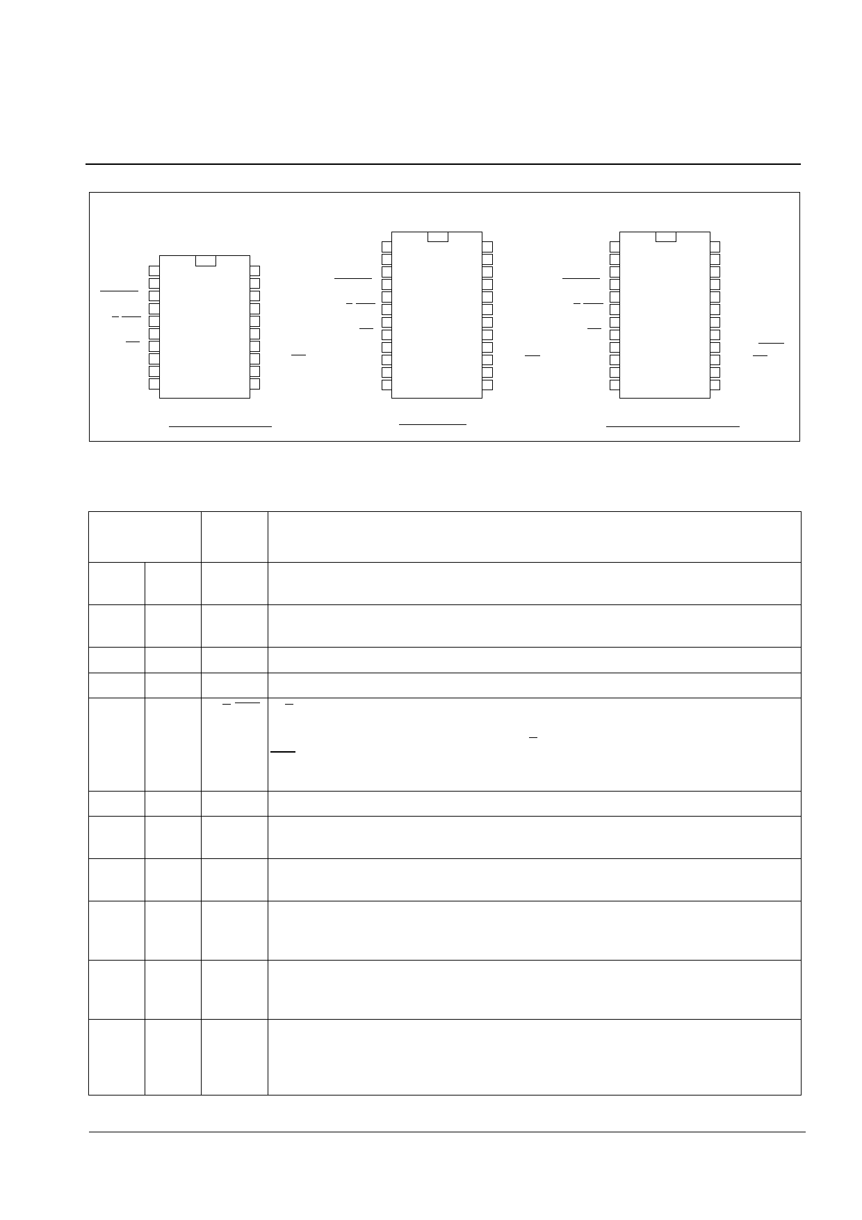
20 PIN SOIC/SSOP
24 PIN PDIP
24 PIN PDIP/SOIC/SSOP
Figure 2 - Pin Connections
Pin Description
Pin #
20 Pin24 Pin
1
1
2
2
3
4
4
5
5
6
6
7
7
8
8
10
9
11
10
12
11
13
Name
Description
VBias Bias Voltage (Output). (VDD/2) volts is available at this pin for biasing external
amplifiers. Connect 0.1 µF capacitor to VSSA.
VRef Reference Voltage for Codec (Output). Used internally. Nominally [Vdd/2 - 1.1]
volts. Connect 0.1 µF capacitor to VSSA.
PWRST Power-up Reset (Input). CMOS compatible input with Schmitt Trigger (active low).
IC Internal Connection. Tie externally to VSSD for normal operation.
A/µ/IRQ A/µ - When internal control bit DEn = 0 this CMOS level compatible input pin governs
the companding law used by the filter/Codec; µ-Law when tied to VSSD and A-Law
when tied to VDD. Logically OR’ed with A/µ register bit.
IRQ - When internal control bit DEn = 1 this pin becomes an open-drain interrupt
output signalling valid access to the D-Channel registers in ST-BUS mode.
VSSD
CS
Digital Ground. Nominally 0 volts.
Chip Select (Input). This input signal is used to select the device for microport
data transfers. Active low. CMOS level compatible.
SCLK Serial Port Synchronous Clock (Input). Data clock for microport. CMOS level
compatible.
DATA 1 Bidirectional Serial Data. Port for microprocessor serial data transfer. In
Motorola/National mode of operation, this pin becomes the data transmit pin only
and data receive is performed on the DATA 2 pin. Input CMOS level compatible.
DATA 2 Serial Data Receive. In Motorola/National mode of operation, this pin is used for
data receive. In Intel mode, serial data transmit and receive are performed on the
DATA 1 pin and DATA 2 is disconnected. Input CMOS level compatible.
Dout Data Output. A high impedance three-state digital output for 8 bit wide channel
data being sent to the Layer 1 transceiver. Data is shifted out via this pin concurrent
with the rising edge of the bit clock during the timeslot defined by STB, or according
to standard ST-BUS timing.
3
Zarlink Semiconductor Inc.
Share Link: 