MCM63P631A 데이터 시트보기 (PDF) - Motorola => Freescale
부품명
상세내역
제조사
MCM63P631A Datasheet PDF : 16 Pages
| |||
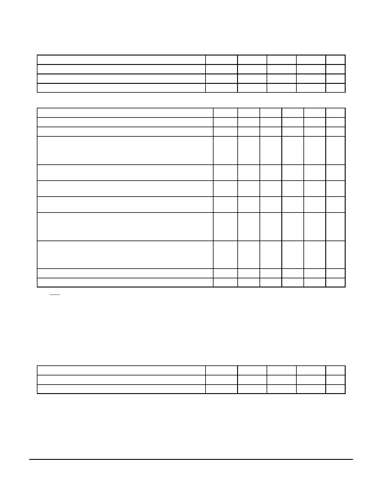
DC OPERATING CONDITIONS AND CHARACTERISTICS
(VDD = 3.3 V + 10%, – 5%, TA = 0 to 70°C, Unless Otherwise Noted)
RECOMMENDED OPERATING CONDITIONS (Voltages Referenced to VSS = 0 V)
Parameter
Symbol
Supply Voltage
Input Low Voltage
Input High Voltage
VDD
VIL
VIH
Min
3.135
– 0.5
2.0
Typ
Max
Unit
3.3
3.6
V
—
0.8
V
—
VDD + 0.5 V
DC CHARACTERISTICS AND SUPPLY CURRENTS
Parameter
Symbol Min
Typ
Max
Input Leakage Current (0 V ≤ Vin ≤ VDD)
Ilkg(I)
—
Output Leakage Current (0 V ≤ Vin ≤ VDD)
Ilkg(O)
—
AC Supply Current (Device Selected, All Outputs Open, MCM63P631A–117 IDDA
—
Freq = Max, VDD = Max)
MCM63P631A–100
—
MCM63P631A–75
—
MCM63P631A–66
—
—
±1
—
±1
—
TBD
—
—
—
CMOS Standby Supply Current (Device Deselected, Freq = 0,
VDD = Max, All Inputs Static at CMOS Levels)
Sleep Mode Supply Current (Sleep Mode, Freq = Max, VDD = Max,
All Other Inputs Static at CMOS Levels, ZZ ≥ VDD – 0.2 V)
TTL Standby (Device Deselected, Freq = 0, VDD = Max,
All Inputs Static at TTL Levels)
ISB2
—
IZZ
—
ISB3
—
—
TBD
—
2
—
TBD
Clock Running (Device Deselected, Freq = Max,
VDD = Max, All Inputs Toggling at CMOS Levels)
MCM63P631A–117 ISB4
—
MCM63P631A–100
—
MCM63P631A–75
—
MCM63P631A–66
—
—
TBD
—
—
—
Static Clock Running (Device Deselected, Freq = Max, MCM63P631A–117 ISB5
—
VDD = Max, All Inputs Static at TTL Levels)
MCM63P631A–100
—
MCM63P631A–75
—
MCM63P631A–66
—
—
TBD
—
—
—
Output Low Voltage (IOL = 8 mA)
VOL
—
—
0.4
Output High Voltage (IOH = – 4 mA)
VOH
2.4
—
—
NOTES:
1. LBO pin has an internal pullup and will exhibit leakage currents of ± 5 µA.
2. ZZ pin has an internal pulldown and will exhibit leakage currents of ± 5 µA.
3. Reference AC Operating Conditions and Characteristics for input and timing (VIH/VIL, tr/tf, pulse level 0 to 3.0 V).
4. All addresses transition simultaneously low (LSB) and then high (MSB).
5. Data states are all zero.
6. Device in Deselected mode as defined by the Truth Table.
7. CMOS levels are Vin ≤ VSS + 0.2 V or ≥ VDD – 0.2 V.
8. Device in Sleep Mode as defined by the Asynchronous Truth Table.
9. TTL levels are Vin ≤ VIL or ≥ VIH.
Unit Notes
µA
1, 2
µA
mA 3, 4, 5
mA
6, 7
mA 2, 7, 8
mA
6, 9
mA
6, 7
mA
6, 9
V
V
CAPACITANCE (f = 1.0 MHz, dV = 3.0 V, TA = 0 to 70°C, Periodically Sampled Rather Than 100% Tested)
Parameter
Symbol
Min
Typ
Input Capacitance
Input/Output Capacitance
Cin
—
3
CI/O
—
6
Max
Unit
5
pF
8
pF
MCM63P631A
8
MOTOROLA FAST SRAM
Share Link: 