MTD2009J 데이터 시트보기 (PDF) - Shindengen
부품명
상세내역
제조사
MTD2009J Datasheet PDF : 2 Pages
| |||
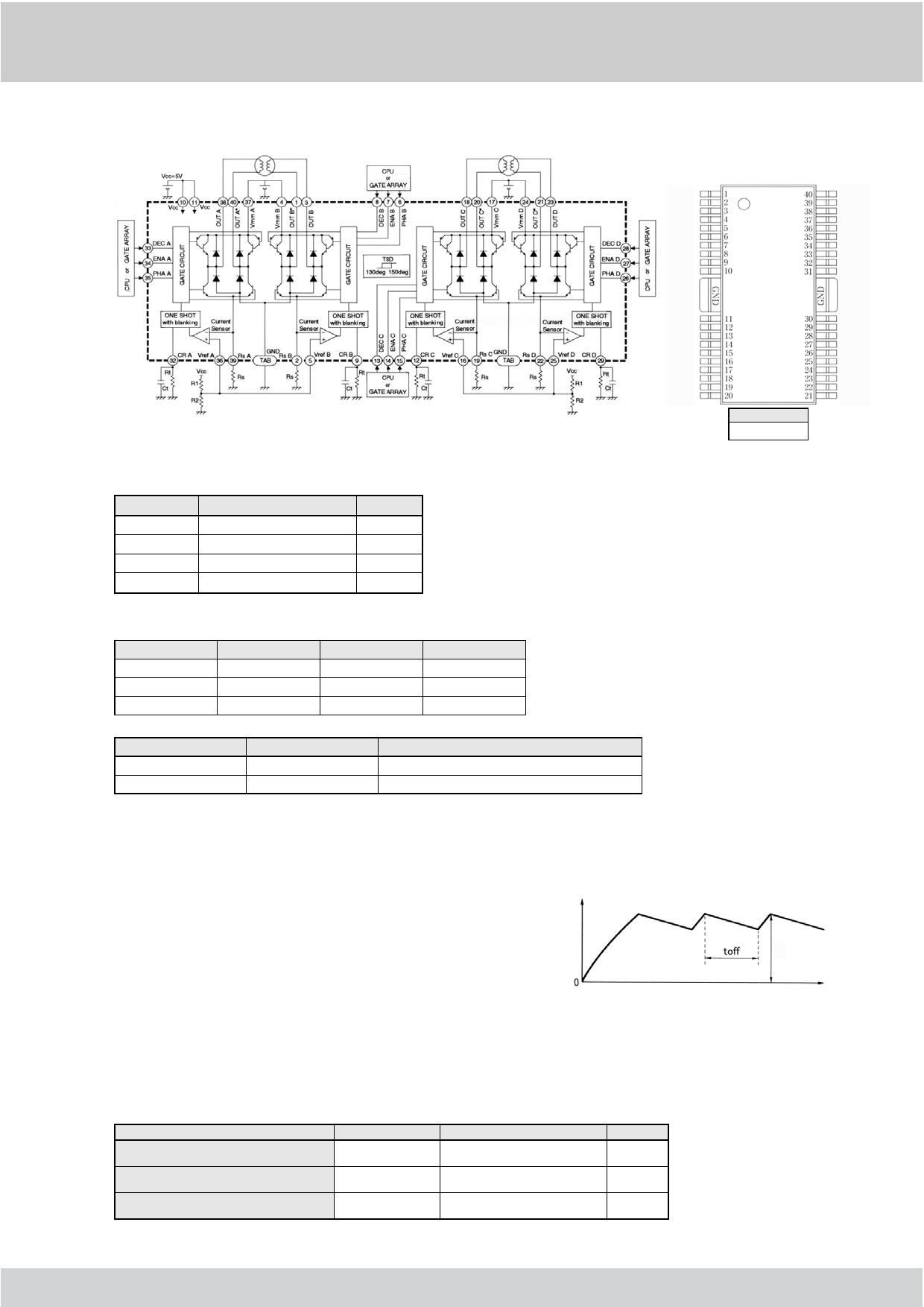
عၮᧄᔕ↪࿁ऍዋ Typical Application
عࡇࡦଙ¾࿑ዋPin Assignment
Top View MTD2009J
OUT B*
Rs B
OUT B
Vmm B
Vref B
PHA B
ENA B
DEC B
CR B
Vcc
OUT A*
Rs A
OUT A
Vmm A
Vref A
PHA A
ENA A
DEC A
CR A
NC
Vcc
CR C
DEC C
ENA C
PHA C
Vref C
Vmm C
OUT C
Rs C
OUT C*
Package
HSOP40
NC
CR D
DEC D
ENA D
PHA D
Vref D
Vmm D
OUT D
Rs D
OUT D*
عផᅑ࿁ऍቯᢙዋ Recommended External Components Value
ܕภޓSymbol
Rs
Rt
Ct
R1+R2
ផᅑ୯ޓRecommendation
0.68
30
1000
҇ 10
නޓUnit
ǡ
kǡ
pF
kǡ
ع⌀ℂ୯؛ዋ Truth Table
ENA A or B or C or D PHA A or B or C or D OUT A or B or C or D OUT A*or B*or C* or D*
L
L
L
H
L
H
H
L
H
፱
፱: don't care
OFF
OFF
DECAY
L
H
Decay Mode
Fast
Slow
Switching Transistor
Both source and sink transistor
Only source transistor
عജชᵹወࡢࡦ࡚ࠪ࠶࠻ࠝࡈᤨശወࡉࡦࠠࡦࠣ࠲ࠗࡓߩܣቯዋ Setting of Output Current,
One Shot Off Time and Blanking Time
٤ ജชᵹܣቯᑼዋ Output Current Setting
lchop Vref 0.012 ᎢAᎤ
Rs
٤ ࡢࡦ࡚ࠪ࠶࠻ࠝࡈᤨശܣቯᑼዋ One Shot Off Time Setting
toff = 1.163 × Ct × Rt ᎢᎺᎤ
Constant current waveform ፯Motor current፰
Ichop
٤ ܣࡓࠗ࠲ࠣࡦࠠࡦࡉቯᑼዋ Blanking Time Setting
ޓtbޓ ޓCޓt × Rޓt × In ⎛⎜⎜⎜⎝ޓ-31----––-----1-1----------00-RR---------00-----tt------00----⎠⎟⎟⎟⎞ ᎢᎺᎤ
عផᅑേ᧦ઙዋ Recommended Operating Conditions
․ߦᜰቯߥ߈႐วߪTa=25͠ዋTa=25͠ unless otherwise specified
ޓ⋡ິParameter
ធวૡ᷷ᐲ
Junction Temperature
ࡠࠫ࠶ࠢชḮช
Logic Supply Voltage
ࡕ࠲ชḮช
Load Supply Voltage
ܕภޓSymbol
Tj
VCC
Vmm
ផᅑ୯ޓRecommendation
-25 ጚ 120
4.75 ጚ 5.25
5 ጚ 31
නޓUnit
͠
V
V
www.shindengen.co.jp/product/semi/
Ķı ዄU170-1ዅ
Share Link: 