MTD6505T 데이터 시트보기 (PDF) - Microchip Technology
부품명
상세내역
제조사
MTD6505T Datasheet PDF : 22 Pages
| |||
MTD6505
1.0 ELECTRICAL
CHARACTERISTICS
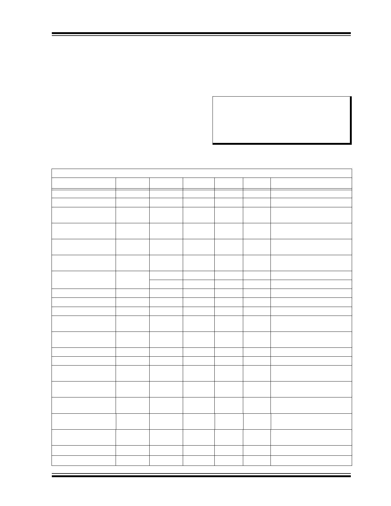
Absolute Maximum Ratings†
Power Supply Voltage (VDD_MAX) ...................... -0.7 to +7.0V
Maximum Output Voltage (VOUT_MAX) ............... -0.7 to +7.0V
Maximum Output Current(1) (IOUT_MAX) ....................1000 mA
FG Maximum Output Voltage (VFG_MAX) ........... -0.7 to +7.0V
FG Maximum Output Current (IFG_MAX) ......................5.0 mA
VBIAS Maximum Voltage (VBIAS_MAX) ................ -0.7 to +4.0V
PWM Maximum Voltage (VPWM_MAX) ................ -0.7 to +7.0V
Allowable Power Dissipation(2)(PD_MAX).........................1.5W
Maximum Junction Temperature (TJ) .......................... +150°C
ESD protection on all pins 2 kV
ELECTRICAL CHARACTERISTICS
† Notice: Stresses above those listed under “Maximum
Ratings” may cause permanent damage to the device.
This is a stress rating only and functional operation of
the device at those or any other conditions above those
indicated in the operational listings of this specification
is not implied. Exposure to maximum rating conditions
for extended periods may affect device reliability.
Note 1: IOUT is also internally limited, according
to the limits defined in the “Electrical
Characteristics” table.
2: Reference Printed Circuit Board (PCB),
according to JEDEC standard EIA/JESD
51-9.
Electrical Specifications: Unless otherwise specified, all limits are established for VDD = 2.0V to 5.5V, TA = +25°C
Parameters
Sym.
Min.
Typ.
Max. Units
Conditions
Power Supply Voltage
VDD
2
Power Supply Current
IVDD
—
Standby Current
IVDD_STB
—
—
5.5
V
5
10
mA VDD = 5V
30
40
µA PWM = 0V, VDD = 5V
(Standby mode)
OUTX
High Resistance
RON(H)
—
0.75
1.1
Ω
IOUT = 0.5A, VDD = 5V
Note 1
OUTX
Low Resistance
RON(L)
—
0.75
1.3
Ω
IOUT = 0.5A, VDD = 5V
Note 1
OUTX
Total Resistance
RON(H+L)
—
1.5
2.4
Ω
IOUT = 0.5A, VDD = 5V
Note 1
VBIAS Internal
Supply Voltage
VBIAS
—
3
—
—
VDD – 0.2
—
V
VDD = 3.2V to 5.5V
V
VDD < 3.2V
PWM Input Frequency
fPWM
1
—
100
kHz
PWM Input H Level
VPWM_H 0.55 VDD
—
VDD
V
VDD 4.5V
PWM Input L Level
VPWM_L
0
—
0.2 VDD
V
VDD 4.5V
PWM Internal Pull-Up
RPWM_0
—
Resistor
266
—
kΩ PWM = 0V
PWM Internal Pull-Up
RPWM
—
Resistor
133
—
kΩ PWM duty-cycle > 0%
DIR Input H Level
VDIR_H VBIAS – 0.5
—
VBIAS
V
VDD 4.5V
DIR Input L Level
VDIR_L
0
—
0.2 VDD
V
VDD 4.5V
DIR Internal Pull-Down
RDIR
100
Resistor
—
200
kΩ
FG Output Pin Low-
VOL_FG
—
Level Voltage
—
0.25
V
IFG = -1 mA
FG Output Pin Leakage ILH_FG
– 10
—
10
µA VFG = 5.5V
Current
Lock Protection
Operating Time
TRUN
—
0.5
—
s
Lock Protection Waiting TWAIT
4.5
Time
5
5.5
s
Note 2
Overcurrent Protection IOC_MOT
—
Overvoltage Protection
VOV
—
750
—
mA Note 3
7.2
—
V
2011-2014 Microchip Technology Inc.
DS20002281C-page 5
Share Link: 