MTD6501C 데이터 시트보기 (PDF) - Microchip Technology
부품명
상세내역
제조사
MTD6501C Datasheet PDF : 24 Pages
| |||
MTD6501C/D/G
1.0 ELECTRICAL
CHARACTERISTICS
Absolute Maximum Ratings†
Power Supply Voltage (VCC_MAX) .................... -0.7 to +15.3V
Maximum OUT1, 2, 3 Output Voltage (VOUT_MAX) .................
................................................................ -0.7 to +15.3V+0.7V
FG Maximum Output Voltage (VFG_MAX) ......... -0.7 to +15.3V
Maximum Output Current(3,4) (IOUT_MAX)....................800 mA
Maximum Output Current(3,5) (IOUT_MAX)....................500 mA
FG Maximum Output Voltage (VFG_MAX) ......... -0.7 to +15.3V
FG Maximum Output Current (IFG_MAX) .....................5.0 mA
VDD Maximum Voltage (VDD_MAX) ..................... -0.7 to +4.0V
PWM Maximum Voltage (VPWM_MAX) ................ -0.7 to +4.0V
Allowable Power Dissipation(1,2,4)(PD_MAX).....................1.0W
Allowable Power Dissipation(1,2,5)(PD_MAX).....................0.5W
Max Junction Temperature (TJ)....................................+150°C
† Notice: Stresses above those listed under “Maximum
Ratings” may cause permanent damage to the device.
This is a stress rating only and functional operation of
the device at those or any other conditions above those
indicated in the operational listings of this specification
is not implied. Exposure to maximum rating conditions
for extended periods may affect device reliability.
Note 1: Reference PCB, according to JEDEC
standard EIA/JESD 51-9.
2: Derating applies for ambient temperatures
outside the specified operating range (refer
to Figure 1-1).
3: OUT1, OUT2, OUT3 (Continuous,
100% duty cycle).
4: MTD6501C and MTD6501G
5: MTD6501D
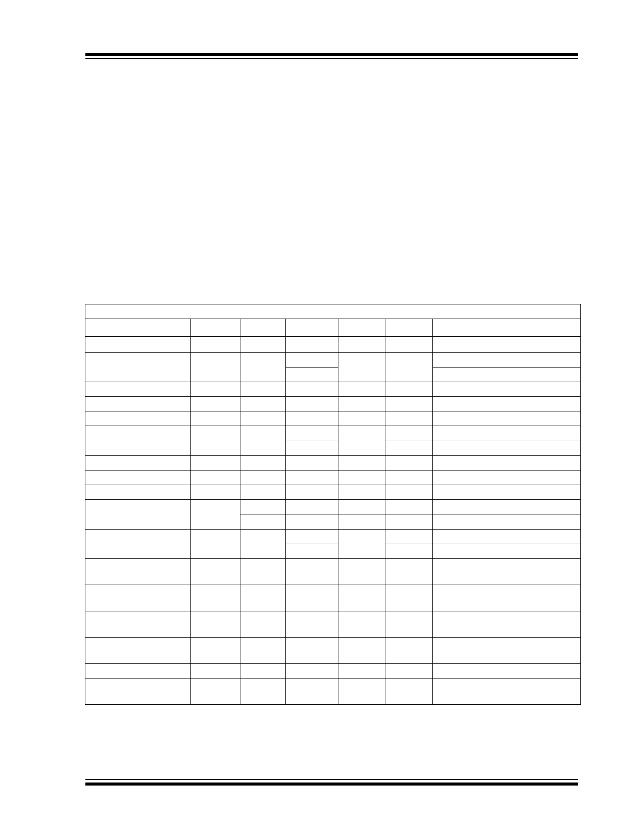
ELECTRICAL CHARACTERISTICS
Electrical Specifications: Unless otherwise specified, all limits are established for VCC = 5.0V, TA = +25°C
Parameters
Sym.
Min.
Typ.
Max.
Units
Conditions
Power Supply Voltage
VCC
2
—
14
V
Power Supply Current
IVCC
—
10
—
mA Rotation Mode
5
Lock-Protection Mode
OUTx High Resistance
OUTx Low Resistance
OUTx Total Resistance
VDD Output Voltage
PWM Input Frequency
PWM Input H Level
PWM Input L Level
PWM Internal Pull-Up
Current
PWM Output
Frequency
FG Output Pin Low
Level Voltage
RON(H)
RON(L)
RON(H+L)
VDD
fPWM
VPWM_H
VPWM_L
IPWM_L
fPWM_O
VOL_FG
—
—
—
—
0.02
0.8*VDD
0
17
8
—
—
0.75
0.75
1.5
3
VCC – 0.2
—
—
—
34
17
20
23
—
1
1
2
—
100
3.6
0.2*VDD
—
—
—
0.25
Ω
IOUT = 0.5A, VCC = 3.3V to 14V
Ω
IOUT = -0.5A, VCC = 3.3V to 14V
Ω
IOUT = 0.5A, VCC = 3.3V to 14V
V
VCC = 3.3V to 14V
V
VCC < 3.3V
kHz
—
V
—
V
—
µA PWM = GND, VCC = 3.3V to 14V
µA PWM = GND, VCC < 3.3V
kHz MTD6501C and MTD6501D
kHz MTD6501G
V
IFG = -1 mA
FG Output Pin Leakage ILH_FG
—
—
10
µA VFG = 14V
Current
Lock Protection
Operating Time
TRUN
—
0.5
—
s
—
Lock Protection Waiting TWAIT
4.5
5
5.5
s
—
Time
Thermal Shutdown
TSD
—
170
—
°C —
Thermal Shutdown
TSD_HYS
—
25
—
°C —
Hysteresis
2010-2012 Microchip Technology Inc.
DS22263B-page 5
Share Link: 