MTP33N10 데이터 시트보기 (PDF) - Motorola => Freescale
부품명
상세내역
제조사
MTP33N10 Datasheet PDF : 8 Pages
| |||
MTP33N10E
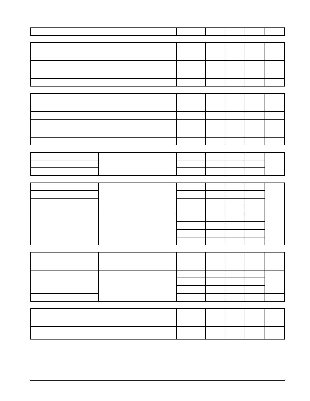
ELECTRICAL CHARACTERISTICS (TJ = 25°C unless otherwise noted)
Characteristic
Symbol
Min
Typ
Max
Unit
OFF CHARACTERISTICS
Drain–Source Breakdown Voltage
(VGS = 0 Vdc, ID = 250 µAdc)
Temperature Coefficient (Positive)
Zero Gate Voltage Drain Current
(VDS = 100 Vdc, VGS = 0 Vdc)
(VDS = 100 Vdc, VGS = 0 Vdc, TJ = – 25°C)
Gate–Body Leakage Current (VGS = ± 20 Vdc, VDS = 0)
ON CHARACTERISTICS (1)
Gate Threshold Voltage
(VDS = VGS, ID = 250 µAdc)
Temperature Coefficient (Negative)
V(BR)DSS
100
—
—
118
—
Vdc
—
mV/°C
IDSS
µAdc
—
—
10
—
—
100
IGSS
—
—
100
nAdc
VGS(th)
2.0
—
4.0
Vdc
—
7.0
—
mV/°C
Static Drain–Source On–Resistance (VGS = 10 Vdc, ID = 16.5 Adc)
Drain–Source On–Voltage (VGS = 10 Vdc)
(ID = 33 Adc)
(ID = 16.5 Adc, TJ = – 25°C)
Forward Transconductance (VDS = 8.0 Vdc, ID = 16.5 Adc)
DYNAMIC CHARACTERISTICS
Input Capacitance
Output Capacitance
Reverse Transfer Capacitance
(VDS = 25 Vdc, VGS = 0 Vdc,
f = 1.0 MHz)
SWITCHING CHARACTERISTICS (2)
Turn–On Delay Time
Rise Time
Turn–Off Delay Time
Fall Time
Gate Charge
(See Figure 8)
(VDD = 50 Vdc, ID = 33 Adc,
VGS = 10 Vdc,
RG = 9.1 Ω)
(VDS = 80 Vdc, ID = 33 Adc,
VGS = 10 Vdc)
SOURCE–DRAIN DIODE CHARACTERISTICS
Forward On–Voltage (1)
(IS = 33 Adc, VGS = 0 Vdc)
(IS = 33 Adc, VGS = 0 Vdc, TJ = 125°C)
RDS(on)
VDS(on)
gFS
Ciss
Coss
Crss
td(on)
tr
td(off)
tf
QT
Q1
Q2
Q3
VSD
—
0.04
0.06
Ohm
Vdc
—
1.6
2.4
—
—
2.1
8.0
—
—
mhos
—
1830
2500
pF
—
678
1200
—
559
1100
—
18
40
ns
—
164
330
—
48
100
—
83
170
—
52
110
nC
—
12
—
—
32
—
—
24
—
Vdc
—
1.0
2.0
—
0.98
—
Reverse Recovery Time
(See Figure 14)
(IS = 33 Adc, VGS = 0 Vdc,
dIS/dt = 100 A/µs)
Reverse Recovery Stored Charge
INTERNAL PACKAGE INDUCTANCE
Internal Drain Inductance
(Measured from contact screw on tab to center of die)
(Measured from the drain lead 0.25″ from package to center of die)
trr
ta
tb
QRR
LD
—
144
—
ns
—
108
—
—
36
—
—
0.93
—
µC
nH
—
3.5
—
4.5
Internal Source Inductance
LS
(Measured from the source lead 0.25″ from package to source bond pad)
(1) Pulse Test: Pulse Width ≤ 300 µs, Duty Cycle ≤ 2%.
(2) Switching characteristics are independent of operating junction temperature.
—
7.5
—
nH
2
Motorola TMOS Power MOSFET Transistor Device Data
Share Link: 