NBSG16VS 데이터 시트보기 (PDF) - ON Semiconductor
부품명
상세내역
제조사
NBSG16VS Datasheet PDF : 14 Pages
| |||
NBSG16VS
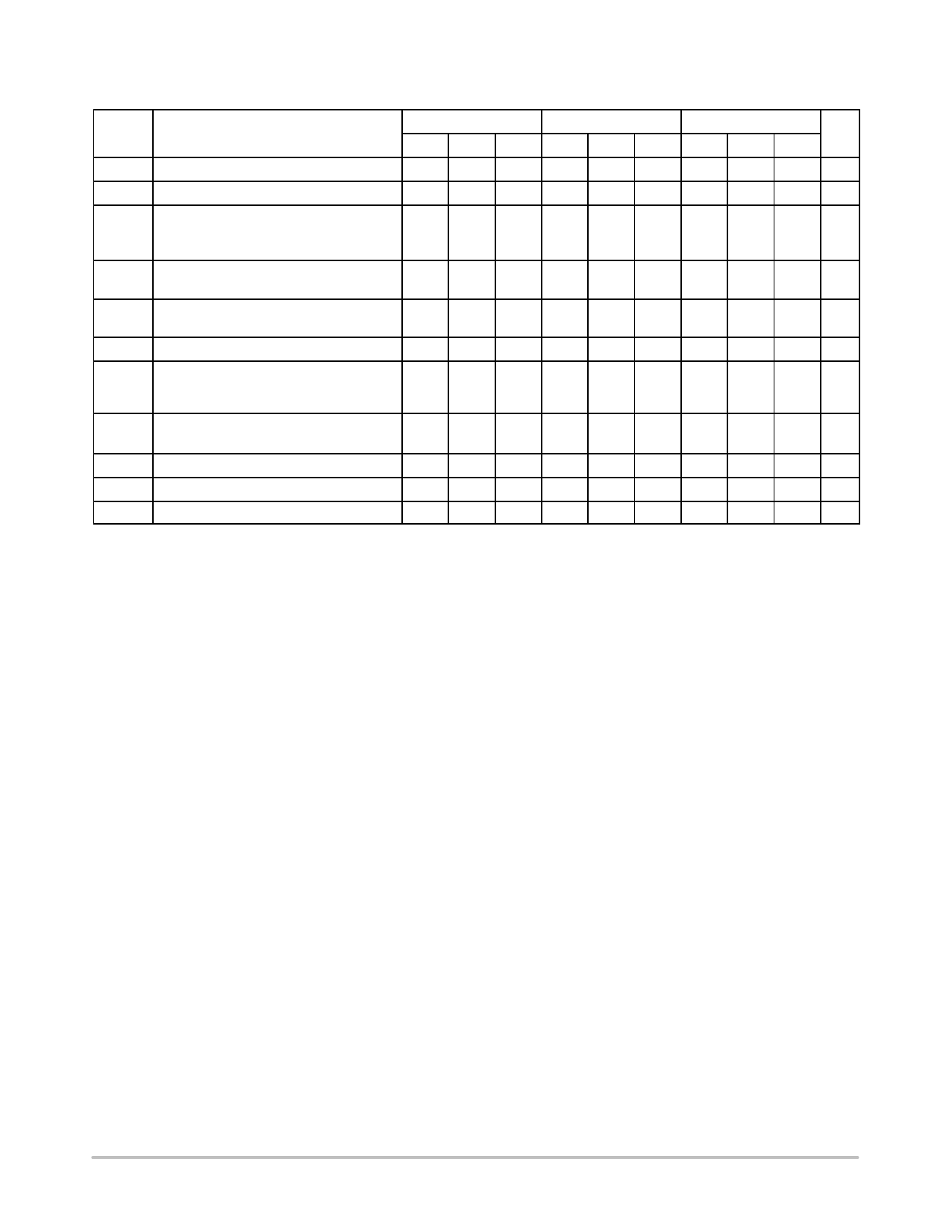
Table 6. DC CHARACTERISTICS, INPUT WITH VARIABLE PECL OUTPUT VCC = 3.3 V; VEE = 0 V (Note 18)
−40°C
25°C
85°C
Symbol
Characteristic
Min Typ Max Min Typ Max Min Typ Max Unit
IEE
Negative Power Supply Current
20
27
34
20
27
34
20
27
34 mA
VOH
Output HIGH Voltage (Note 13)
2095 2220 2345 2085 2210 2335 2075 2200 2325 mV
VOL
Output LOW Voltage (Note 13)
mV
(Max Swing) 1275 1395 1515 1285 1405 1525 1295 1415 1535
(VCTRL = VCC − 600 mV) 1750 1870 1990 1730 1850 1970 1715 1835 1955
VIH
Input HIGH Voltage
(Single−Ended) (Notes 15 and 16)
VTHR VCC − VCC VTHR VCC − VCC VTHR VCC − VCC mV
+ 75 1000*
+ 75 1000*
+ 75 1000*
VIL
Input LOW Voltage
(Single−Ended) (Notes 15 and 17)
VIH − VCC − VTHR VIH − VCC − VTHR VIH − VCC − VTHR mV
2500 1400* − 75 2500 1400* − 75 2500 1400* − 75
VBB
VIHCMR
PECL Output Voltage Reference
Input HIGH Voltage Common Mode
Range (Note 14)
(Differential Configuration)
1880 1940 2000 1880 1940 2000 1880 1940 2000 mV
1.2
3.3 1.2
3.3 1.2
3.3 V
VMM
RTIN
IIH
IIL
CMOS Output Voltage Reference
mV
(VCC − VEE)/2 1500 1650 1800 1500 1650 1800 1500 1650 1800
Internal Input Termination Resistor
45
50
55
45
50
55
45
50
55
W
Input HIGH Current (@ VIH)
Input LOW Current (@ VIL)
30 100
25
50
30 100
25
50
30 100 mA
25
50 mA
NOTE: Device will meet the specifications after thermal equilibrium has been established when mounted in a test socket or printed circuit
board with maintained transverse airflow greater than 500 lfpm. Electrical parameters are guaranteed only over the declared
operating temperature range. Functional operation of the device exceeding these conditions is not implied. Device specification limit
values are applied individually under normal operating conditions and not valid simultaneously.
*Typicals used for testing purposes.
13. All loading with 50 W to VCC − 2.0 V. VOH/VOL measured at VIH/VIL.
14. VIHCMR min varies 1:1 with VEE, VIHCMR max varies 1:1 with VCC. The VIHCMR range is referenced to the most positive side of the differential
input signal.
15. VTHR is the voltage applied to the complementary input, typically VBB or VMM. VTHR(MIN) = VIHCMR + 75 mV. VTHR(MAX) = VIHCMR − 75 mV.
16. VIH cannot exceed VCC.
17. VIL always w VEE.
18. Input and output parameters vary 1:1 with VCC. VEE can vary +0.925 V to −0.165 V.
http://onsemi.com
6
Share Link: 