NCP1417 데이터 시트보기 (PDF) - ON Semiconductor
부품명
상세내역
제조사
NCP1417 Datasheet PDF : 13 Pages
| |||
NCP1417
higher than 1.190 V + 30 mV, the comparator output will
cause the 50 W low side switch to be turned OFF, pin 3 will
become high impedance, and its voltage will be pulled high.
The second low−battery detector functions in the same
manner, the second comparator, CP2 with a lower triggering
reference point derived from the internal reference is used
instead, typical 0.944 V. This configuration provides two
levels of low battery warning to the target system.
APPLICATIONS INFORMATION
Output Voltage Setting
The output voltage of the converter is determined by the
external feedback network comprised of RFB1 and RFB2 and
the relationship is given by:
ǒ Ǔ VOUT + 1.190 V
1
)
RFB1
RFB2
where RFB1 and RFB2 are the upper and lower feedback
resistors respectively.
Low Battery Detect Level Setting
The Low Battery Detect Voltages of the converter are
determined by the external divider network comprised of
RLB1 and RLB2 and the relationship is given by:
ǒ Ǔ VLB1 + 1.190 V
1
)
RLB1
RLB2
where RLB1 and RLB2 are the upper and lower divider
resistors respectively. By setting the VLB1, the second low
battery detection point, VLB2 will be fixed automatically.
Inductor Selection
The NCP1417 is tested to produce optimum performance
with a 22 mH inductor at VIN = 3.0 V, VOUT = 3.3 V
supplying output current up to 200 mA. For other
input/output requirements, inductance in the range 10 mH to
47 mH can be used according to end application
specifications. Selecting an inductor is a compromise
between output current capability and tolerable output
voltage ripple. Of course, the first thing we need to obey is
to keep the peak inductor current below its saturation limit
at maximum current and the ILIM of the device. In NCP1417,
ILIM is set at 1.0 A. As a rule of thumb, low inductance
values supply higher output current, but also increase the
ripple at output and reducing efficiency, on the other hand,
high inductance values can improve output ripple and
efficiency, however it also limit the output current capability
at the same time. One other parameter of the inductor is its
DC resistance, this resistance can introduce unwanted
power loss and hence reduce overall efficiency, the basic
rule is selecting an inductor with lowest DC resistance
within the board space limitation of the end application.
Capacitors Selection
In all switching mode boost converter applications,
both the input and output terminals sees impulsive
voltage/current waveforms. The currents flowing into and
out of the capacitors multiplying with the Equivalent Series
Resistance (ESR) of the capacitor producing ripple voltage
at the terminals. During the syn−rect switch off cycle, the
charges stored in the output capacitor is used to sustain the
output load current. Load current at this period and the ESR
combined and reflected as ripple at the output terminal. For
all cases, the lower the capacitor ESR, the lower the ripple
voltage at output. As a general guide line, low ESR
capacitors should be used. Ceramic capacitors have the
lowest ESR, but low ESR tantalum capacitors can also be
used as a cost effective substitute.
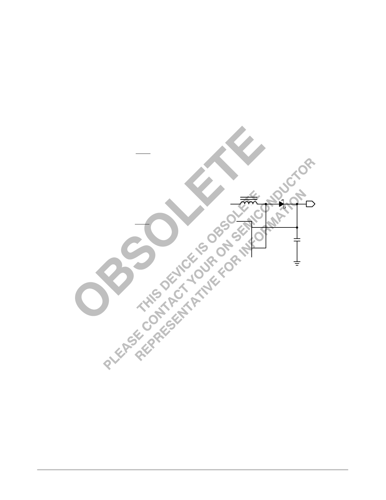
Optional Startup Schottky Diode for Low Battery
Voltage
In general operation, no external schottky diode is
required, however, in case you are intended to operate the
device close to 1.0 V level, a schottky diode connected
between the LX and OUT pins as shown in Figure 27 can
help during startup of the converter. The effect of the
additional schottky is shown in Figure 8.
MBR0520
L
VOUT
OUT
NCP1417
LX
COUT
Figure 27.
PCB Layout Recommendations
Good PCB layout plays an important role in switching
mode power conversion. Careful PCB layout can help to
minimize ground bounce, EMI noise and unwanted
feedback that can affect the performance of the converter.
Hints suggested in below can be used as a guide line in most
situations.
Grounding
Star−ground connection should be used to connect the
output power return ground, the input power return ground
and the device power ground together at one point. All high
current running paths must be thick enough for current
flowing through and producing insignificant voltage drop
along the path. Feedback signal path must be separated with
the main current path and sensing directly at the anode of the
output capacitor.
Components Placement
Power components, i.e. input capacitor, inductor and
output capacitor, must be placed as close together as
possible. All connecting traces must be short, direct and
thick. High current flowing and switching paths must be
http://onsemi.com
10
Share Link: 