NCP1417 데이터 시트보기 (PDF) - ON Semiconductor
부품명
상세내역
제조사
NCP1417 Datasheet PDF : 13 Pages
| |||
NCP1417
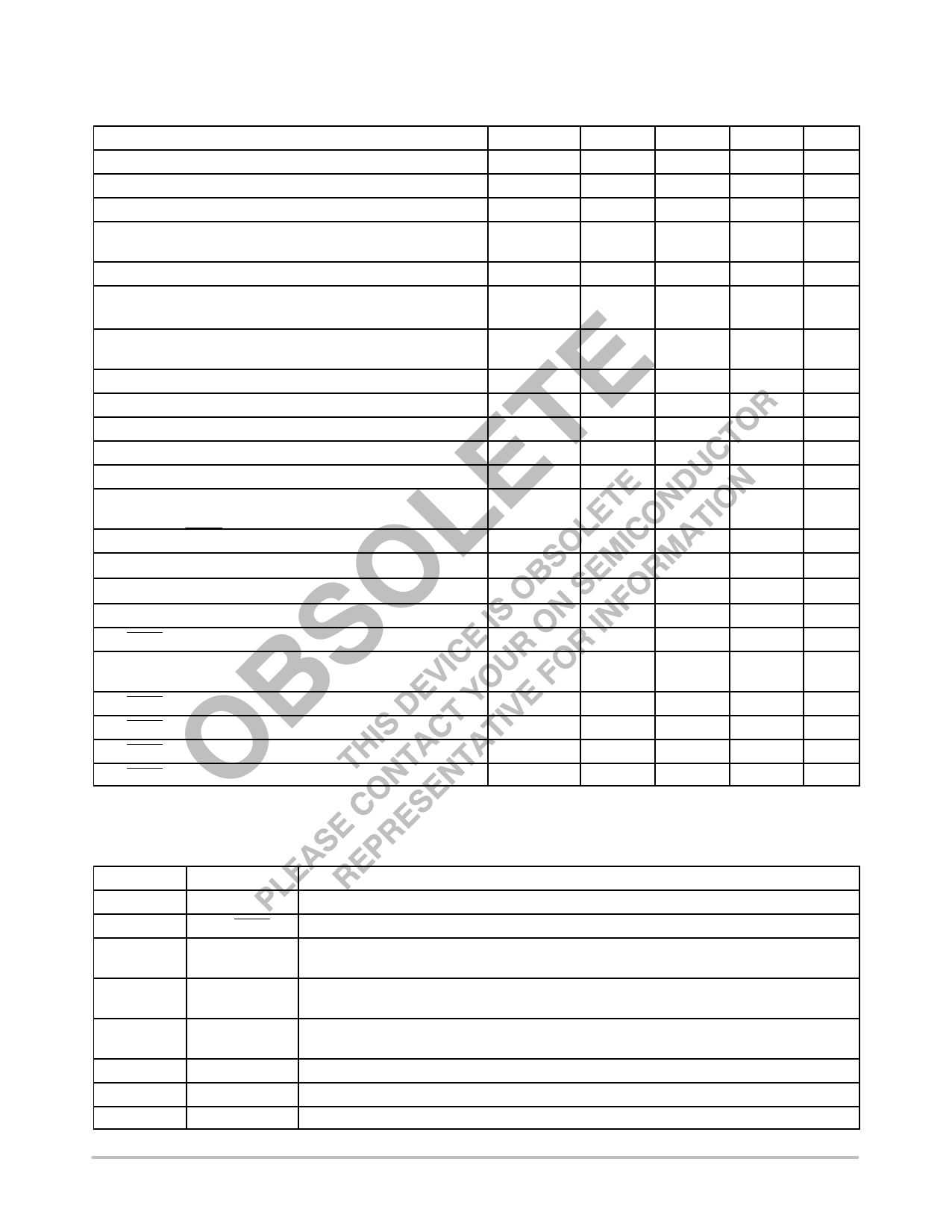
ELECTRICAL CHARACTERISTICS (VOUT = 3.3 V, TA = 25°C for typical value, −40°C ≤ TA ≤ 85_C for min/max values unless
otherwise noted.)
Characteristics
Symbol
Min
Typ
Max
Unit
Operating Voltage
Output Voltage Range (Adjusted by External Feedback)
Reference Voltage (CREF = 150 nF, Under No Loading, TA = 25_C)
Reference Voltage (CREF = 150 nF, Under No Loading,
−40_C ≤ TA ≤ 85_C)
Reference Voltage Temperature Coefficient
Reference Voltage Load Current
(VOUT = 3.3 V, VREF = VREF_NL " 1.5%, CREF = 1.0 mF) (Note 5)
VIN
VOUT
VREF_NL
VREF_NL_A
TCVREF
IREF
1.0
VIN
1.183
1.178
−
2.5
−
−
1.190
−
0.03
−
5.5
V
5.5
V
1.197
V
1.202
V
−
mV/_C
−
mA
Reference Voltage Load Regulation
(VOUT = 3.3 V, ILOAD = 0 to 100 mA, CREF = 1.0 mF)
VREF_LOAD
−
0.015
1.0
mV
Reference Voltage Line Regulation
FB, LBI Input Threshold
Internal NFET ON−Resistance (ILX = 100 mA)
Internal PFET ON−Resistance (ILX = 100 mA)
LX Switch Current Limit (NFET)
Operating Current into OUT
(VFB = 1.4 V, i.e. No Switching, VOUT = 3.3 V)
VREF_LINE
VFB, VLBI
RDS(ON)_N
RDS(ON)_P
ILIM
IQ
−
1.172
−
−
−
−
0.03
1.190
0.65
1.3
1.0
9.0
1.0
1.200
−
−
−
14
mV/V
V
W
W
A
mA
Shutdown Current into OUT (SHDN = GND)
LX Switch MAX. ON−Time (VFB = 1.0 V, VOUT = 3.3 V)
LX Switch MIN. OFF−Time (VFB = 1.0 V, VOUT = 3.3 V)
FB Input Current
LBI/SHDN Input Current
LBO1/LBO2 Low Output Voltage (VLBI = 0, ISINK = 1.0 mA)
ISD
tON
tOFF
IFB
ILBI, ISHDN
VLBO_L1
VLBO_L2
−
0.8
0.22
−
−
−
−
0.05
1.4
0.25
1.5
1.5
−
−
1.0
mA
2.0
mS
0.46
mS
20
nA
8.0
nA
0.08
V
0.08
LBI/SHDN Input Threshold for LBO1
LBI/SHDN Input Threshold for LBO2
LBI/SHDN Input Threshold, Low
LBI/SHDN Input Threshold, High
5. Loading capability decreases with VOUT.
VLBI1
1.172
1.190
1.200
V
VLBI2
0.904
0.944
0.965
V
VSHDN_L
−
−
0.3
V
VSHDN_H
0.6
−
−
V
PIN FUNCTION DESCRIPTION
Pin No.
Pin Name
Pin Description
1
FB
Output Voltage Feedback Input.
2
LBI/SHDN
Low−Battery Detector Input and Shutdown Control input multi−function pin.
3
LBO1
Open−Drain Low−Battery Detector Output. Output is LOW when VLBI is < 1.172 V. LBO1 is high
impedance during shutdown.
4
REF
1.190 V Reference Voltage Output, bypassing with 150 nF capacitor if this pin is not loaded,
bypassing with 1 μF if this pin is loaded up to 2.5 mA @ VOUT = 3.3 V.
5
LBO2
Open−Drain Low−Battery Detector Output. Output is LOW when VLBI is < 0.904 V. LBO2 is high
impedance during shutdown.
6
GND
Ground
7
LX
N−Channel and P−Channel Power MOSFET Drain Connection.
8
OUT
Power Output. OUT provides bootstrap power to the IC.
http://onsemi.com
3
Share Link: 