NE1617A 데이터 시트보기 (PDF) - Philips Electronics
부품명
상세내역
제조사
NE1617A Datasheet PDF : 17 Pages
| |||
Philips Semiconductors
Temperature monitor for microprocessor systems
Product data sheet
NE1617A
SMBus INTERFACE AC SPECIFICATIONS1
VDD = 3.0 V to 3.6 V2; Tamb = 0 _C to +125 _C unless otherwise noted.
These specifications are guaranteed by design and not tested in production.
SYMBOL
PARAMETER
CONDITIONS
MIN
TYP
ÁÁÁÁÁÁÁÁÁÁÁÁÁÁÁÁÁÁÁÁÁÁÁÁÁÁÁÁÁÁÁÁÁÁ VIH
Logic input high voltage for STBY, SCLK, SDATA
VDD = 3 V to 5.5 V
2.2
ÁÁÁÁÁÁÁÁÁÁÁÁÁÁÁÁÁÁÁÁÁÁÁÁÁÁÁÁÁÁÁÁÁÁ VIL
Logic input low voltage for STBY, SCLK, SDATA
VDD = 3 V to 5.5 V
ÁÁÁÁÁÁÁÁÁÁÁÁÁÁÁÁÁÁÁÁÁÁÁÁÁÁÁÁÁÁÁÁÁÁ IOL
Logic output low sink current for
ÁÁÁÁÁÁÁÁÁÁÁÁÁÁÁÁÁÁÁÁÁÁÁÁÁÁÁÁÁÁÁÁÁÁ ALERT
SDATA
VOL = 0.4 V
1.0
VOL = 0.6 V
6.0
ÁÁÁÁÁÁÁÁÁÁÁÁÁÁÁÁÁÁÁÁÁÁÁÁÁÁÁÁÁÁÁÁÁÁ IIH & IIL
ÁÁÁÁÁÁÁÁÁÁÁÁÁÁÁÁÁÁÁÁÁÁÁÁÁÁÁÁÁÁÁÁÁÁ CIN
ÁÁÁÁÁÁÁÁÁÁÁÁÁÁÁÁÁÁÁÁÁÁÁÁÁÁÁÁÁÁÁÁÁÁ fSCLK
ÁÁÁÁÁÁÁÁÁÁÁÁÁÁÁÁÁÁÁÁÁÁÁÁÁÁÁÁÁÁÁÁÁÁ tLOW
ÁÁÁÁÁÁÁÁÁÁÁÁÁÁÁÁÁÁÁÁÁÁÁÁÁÁÁÁÁÁÁÁÁÁ tHIGH
ÁÁÁÁÁÁÁÁÁÁÁÁÁÁÁÁÁÁÁÁÁÁÁÁÁÁÁÁÁÁÁÁÁÁÁÁÁÁÁÁÁÁÁÁÁÁÁÁÁÁÁÁÁÁÁÁÁÁÁÁÁÁÁÁÁÁÁÁ tBUF
Logic input current
SMBus input capacitance for SCLK,SDATA
SCLK operating frequency
SCLK low time
SCLK high time
SMBus free time.
Delay from SDA stop to SDA start
VIN = VDD or GND
–1.0
5
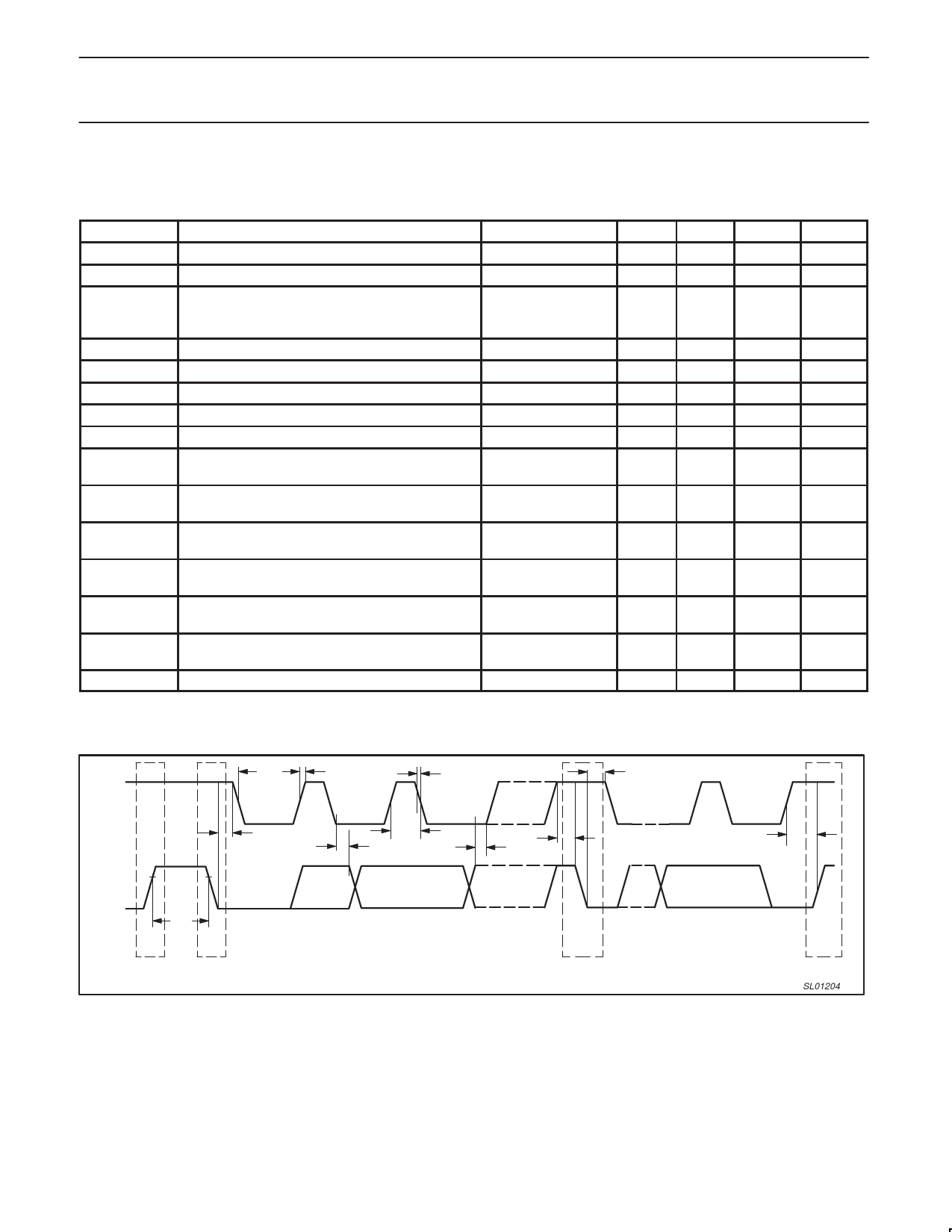
See Figure 4
0
See Figure 4
4.7
5.0
See Figure 4
4.0
5.0
See Figure 4
4.7
ÁÁÁÁÁÁÁÁÁÁÁÁÁÁÁÁÁÁÁÁÁÁÁÁÁÁÁÁÁÁÁÁÁÁ tHD:STA
Hold time of start condition.
Delay from SDA start to first SCL H–L
See Figure 4
4.0
ÁÁÁÁÁÁÁÁÁÁÁÁÁÁÁÁÁÁÁÁÁÁÁÁÁÁÁÁÁÁÁÁÁÁÁÁÁÁÁÁÁÁÁÁÁÁÁÁÁÁÁÁÁÁÁÁÁÁÁÁÁÁÁÁÁÁÁÁ tHD:DAT
Hold time of data.
Delay from SCL H–L to SDA edges
See Figure 4
0
ÁÁÁÁÁÁÁÁÁÁÁÁÁÁÁÁÁÁÁÁÁÁÁÁÁÁÁÁÁÁÁÁÁÁ tSU:DAT
Set-up time of data.
Delay from SDA edges to SCL L–H
See Figure 4
250
ÁÁÁÁÁÁÁÁÁÁÁÁÁÁÁÁÁÁÁÁÁÁÁÁÁÁÁÁÁÁÁÁÁÁÁÁÁÁÁÁÁÁÁÁÁÁÁÁÁÁÁÁÁÁÁÁÁÁÁÁÁÁÁÁÁÁÁÁ tSU:STA
Set-up time of repeat start condition.
Delay from SCL L–H to restart SDA
See Figure 4
250
ÁÁÁÁÁÁÁÁÁÁÁÁÁÁÁÁÁÁÁÁÁÁÁÁÁÁÁÁÁÁÁÁÁÁ tSU:STO
Set-up time of stop condition.
Delay from SCL L–H to SDA stop
See Figure 4
4.0
ÁÁÁÁÁÁÁÁÁÁÁÁÁÁÁÁÁÁÁÁÁÁÁÁÁÁÁÁÁÁÁÁÁÁÁÁÁÁÁÁÁÁÁÁÁÁÁÁÁÁÁÁÁÁÁÁÁÁÁÁÁÁÁÁÁÁÁÁ tF
Fall time of SCL and SDA
See Figure 4
MAX
0.8
1.0
100
1.0
UNIT
V
V
mA
mA
µA
pF
kHz
µs
µs
µs
µs
ns
ns
ns
µs
µs
NOTES:
1. The NE1617A does not include the SMBus timeout capability (tLOW:SEXT and tLOW:MEXT).
2. Device operation between 3.0 V to 5.5 V is allowed, but parameters may be outside the limit shown in table.
SCLK
tLOW
tR
tHD:STA
tHD:DAT
tF
tHIGH
tSU:DAT
tSU:STA
tHD:STA
tSU:STO
SDATA
tBUF
P
S
S
Figure 4. Timing measurements.
P
SL01204
2004 Oct 05
6
Share Link: 