NE5230 데이터 시트보기 (PDF) - Philips Electronics
부품명
상세내역
제조사
NE5230 Datasheet PDF : 17 Pages
| |||
Philips Semiconductors
Low voltage operational amplifier
Product specification
NE/SA5230
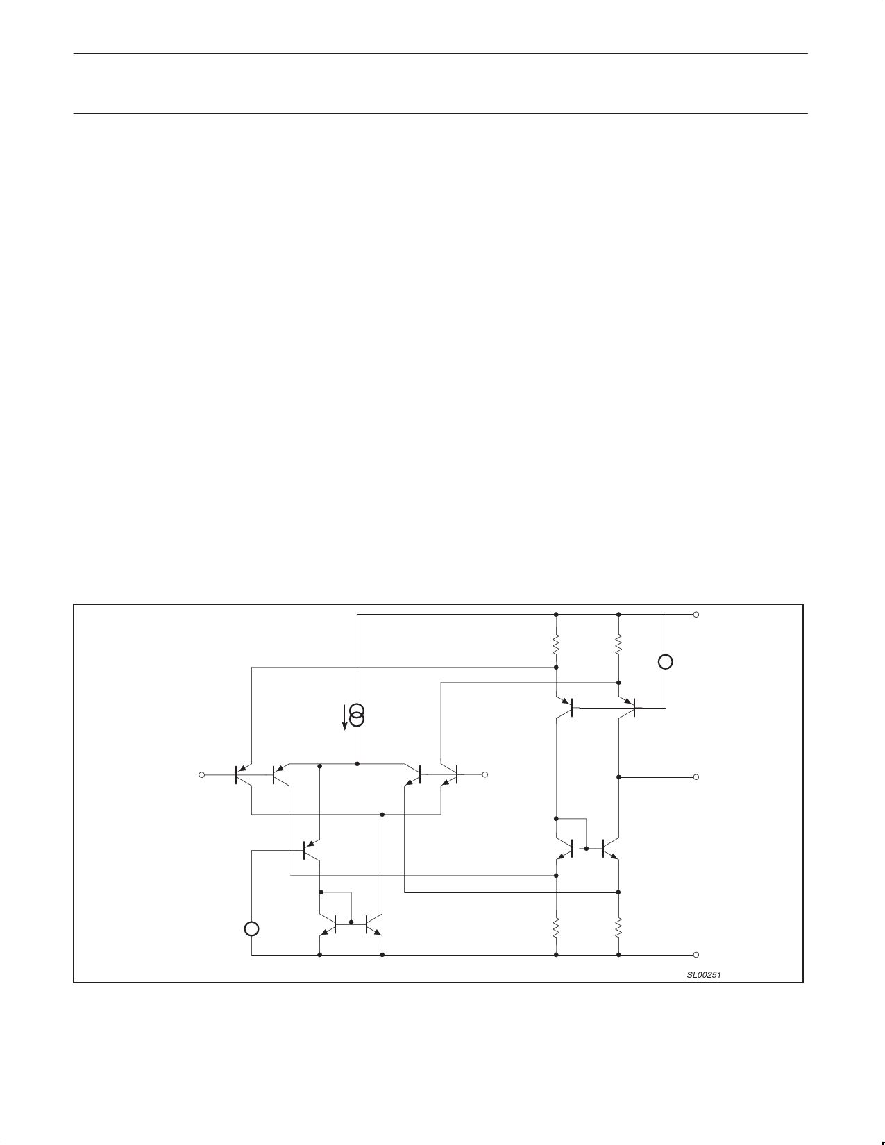
THEORY OF OPERATION
Input Stage
Operational amplifiers which are able to function at minimum supply
voltages should have input and output stage swings capable of
reaching both supply voltages within a few millivolts in order to
achieve ease of quiescent biasing and to have maximum
input/output signal handling capability. The input stage of the
NE5230 has a common-mode voltage range that not only includes
the entire supply voltage range, but also allows either supply to be
exceeded by 250mV without increasing the input offset voltage by
more than 6mV. This is unequalled by any other operational
amplifier today.
In order to accomplish the feat of rail-to-rail input common-mode
range, two emitter-coupled differential pairs are placed in parallel so
that the common-mode voltage of one can reach the positive supply
rail and the other can reach the negative supply rail. The simplified
schematic of Figure 2 shows how the complementary
emitter-coupler transistors are configured to form the basic input
stage cell. Common-mode input signal voltages in the range from
0.8V above VEE to VCC are handled completely by the NPN pair, Q3
and Q4, while common-mode input signal voltages in the range of
VEE to 0.8V above VEE are processed only by the PNP pair, Q1 and
Q2. The intermediate range of input voltages requires that both the
NPN and PNP pairs are operating. The collector currents of the
input transistors are summed by the current combiner circuit
composed of transistors Q8 through Q11 into one output current.
Transistor Q8 is connected as a diode to ensure that the outputs of
Q2 and Q4 are properly subtracted from those of Q1 and Q3.
Ib1
The input stage was designed to overcome two important problems
for rail-to-rail capability. As the common-mode voltage moves from
the range where only the NPN pair was operating to where both of
the input pairs were operating, the effective transconductance would
change by a factor of two. Frequency compensation for the ranges
where one input pair was operating would, of course, not be optimal
for the range where both pairs were operating. Secondly, fast
changes in the common-mode voltage would abruptly saturate and
restore the emitter current sources, causing transient distortion.
These problems were overcome by assuring that only the input
transistor pair which is able to function properly is active. The NPN
pair is normally activated by the current source IB1 through Q5 and
the current mirror Q6 and Q7, assuming the PNP pair is
non-conducting. When the common-mode input voltage passes
below the reference voltage, VB1=0.8V at the base of Q5, the
emitter current is gradually steered toward the PNP pair, away from
the NPN pair. The transfer of the emitter currents between the
complementary input pairs occurs in a voltage range of about
120mV around the reference voltage VB1. In this way the sum of the
emitter currents for each of the NPN and PNP transistor pairs is kept
constant; this ensures that the transconductance of the parallel
combination will be constant, since the transconductance of bipolar
transistors is proportional to their emitter currents.
An essential requirement of this kind of input stage is to minimize
the changes in input offset voltage between that of the NPN and
PNP transistor pair which occurs when the input common-mode
voltage crosses the internal reference voltage, VB1. Careful circuit
layout with a cross-coupled quad for each input pair has yielded a
typical input offset voltage of less than 0.3mV and a change in the
input offset voltage of less than 0.1mV.
VCC
R10
R11
+
V
Vb2
Q10
Q11
VIN–
Q3
Q1
Q2 Q4
VIN+
IOUT
Q5
Q8
Q9
+
V
Vb1
Q6
Q7
Figure 2. Input Stage
R8
R9
VEE
SL00251
1994 Aug 31
6
Share Link: 