NJM3773 데이터 시트보기 (PDF) - Japan Radio Corporation
부품명
상세내역
제조사
NJM3773 Datasheet PDF : 9 Pages
| |||
NJM3773
Current sense filtering
At turn-on a current spike occurs, due to the recovery of the recirculation diodes and the capacitance of the motor
winding. To prevent this spike from reseting the flip-flops through the current sensing comparators, the clock
oscillator generates a blanking pulse at turn-on. The blanking pulse disables the comparators for a short time.
Thereby any voltage transient across the sensing resistor will be ignored during the blanking time.
Choose the blanking pulse time to be longer than the duration of the switching transients by selecting a proper CT
value. The time is calculated as:
t = 210 • C [s]
b
T
As the CT value may vary from approximately 2 200 pF to 33 000 pF, a blanking time ranging from 0.5 µs to 7 µs is
possible. Nominal value is 4 700 pF, which gives a blanking time of 1.0 µs.
As the filtering action introduces a small delay, the peak value across the sensing resistor, and hence the peak
motor current, will reach a slightly higher level than what is defined by the reference voltage. The filtering delay
also limits the minimum possible output current. As the output will be on for a short time each cycle, equal to the
digital filtering blanking time plus additional internal delays, an amount of current will flow through the winding.
Typically this current is 1-10 % of the maximum output current set by RS.
Sometimes it may be necessary to include an external in the feed back loop, the filtering may be done by adding
an external low pass filter in series with the comparator C input. In this case the digital blanking time should be as
short as possible. The recommended filter component values are 1 kohm and 820 pF.
To create an absolute zero current, the Dis input should be HIGH.
Switching frequency
The frequency of the clock oscillator is set by the timing components R and C at the RC-pin. As C sets the digital
T
T
T
filter blanking time, the clock oscillator frequency is adjusted by RT. The value of RT is limited to 2 - 20 kohm. The
frequency is approximately calculated as:
f = 1 / ( 0.77 • R • C )
s
T
T
Nominal component values of 12 kohm and 4 700 pF results in a clock frequency of 23.0 kHz. A lower frequency
will result in higher current ripple, but may improve low level linearity. A higher clock frequency reduces current
ripple, but increases the switching losses in the IC and possibly the iron losses in the motor.
Phase inputs
A logic HIGH on a Phase input gives a current flowing from pin M into pin M . A logic LOW gives a current flow in
A
B
the opposite direction. A time delay prevents cross conduction in the H-bridge when changing the Phase input.
Dis (Disable) inputs
A logic HIGH on the Dis inputs will turn off all four transistors of the output H-bridge, which results in a rapidly
decreasing output current to zero.
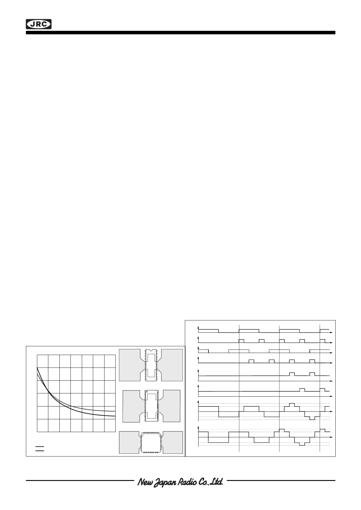
Thermal resistance [°C/W]
80
70
22-pin
DIP
60
50
40
24-pin
EMP
30
20
5
10 15 20 25 30 35
PCB copper foil area [cm2]
PLCC package
DIP package
28-pin
PLCC
Figure 8. Typical thermal resistance vs. PC
Board copper area and suggested layout
Phase 1
Dis 1
Phase 2
Dis 2
V R1
140%
100%
V R2
140%
100%
I MA1
140%
100%
–100%
–140%
I MA2
140%
100%
–100%
–140%
Full step mode
Half step mode
Figure 9. Stepping modes
Modified half step mode
Share Link: 