NJM3777 데이터 시트보기 (PDF) - Japan Radio Corporation
부품명
상세내역
제조사
NJM3777 Datasheet PDF : 10 Pages
| |||
NJM3777
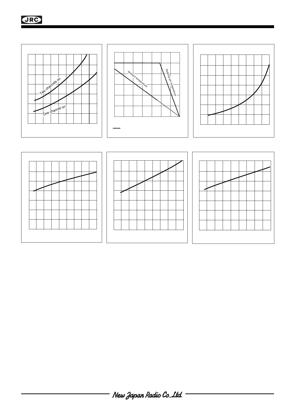
s TYPICAL CHARACTERISTICS
PD (W)
3.0
2.0
Two channels on
1.0
One channel on
0
0
0.20
0.40
0.60
0.80
I M (A)
Figure 10. Power dissipation vs.
motor current.Ta = 25°C
Vd, ld (V)
Maximum allowable power dissipation [W]
6
VCE Sat (V)
5
1.2
4
3
Ambient temperature
1.0
0.8
2
0.6
1
0.4
0
-25
0
25 50 75 100 125 150
Temperature [°C]
EMP package
All ground pins soldered onto a
20 cm2 PCB copper area with
free air convection.
Figure 11. Maximum allowable power
dissipation
0.2
0
0
0.20
0.40
0.60
0.80
I M (A)
Figure 12. Typical lower transistor
saturation voltage vs. output current
VCE Sat (V)
Vd, ud (V)
1.2
1.0
0.8
0.6
0.4
0.2
0
0
0.20
0.40
0.60
0.80
I M (A)
Figure 13. Typical lower diode
voltage drop vs. recirculating
current
1.2
1.2
1.0
1.0
0.8
0.8
0.6
0.6
0.4
0.4
0.2
0.2
0
0
0.20
0.40
0.60
0.80
I M (A)
Figure 14. Typical upper transistor
saturation voltage vs. output current
0
0
0.20
0.40
0.60
0.80
I M (A)
Figure 15. Typical upper diode
voltage drop vs. recirculating current
The specifications on this databook are only
given for information , without any guarantee
as regards either mistakes or omissions.
The application circuits in this databook are
described only to show representative
usages of the product and not intended for
the guarantee or permission of any right
including the industrial rights.
Share Link: 