NJU7327 데이터 시트보기 (PDF) - Japan Radio Corporation
부품명
상세내역
제조사
NJU7327 Datasheet PDF : 7 Pages
| |||
NJU7327
Given that the bias current is set to be 5mA by HW101A datasheet, R1 and R2 can be determined as follows:
R1 +
R2 +
Rin
=
VDD
Ihbias
=
12
5 ×10−3
=
2.4kΩ
R1 = R2 = 1kΩ
The output voltage of hall elements is influenced by the bias current and magnetic flux density of hall elements.
The optimum input voltage of NJU7327 is 100mVp-p and higher. With such input voltage, the highest efficiency can
be obtained.
4. Design of FG output resistance (R3)
FG Out (FG: Pin8) is an open drain output and R3 is a pull up register. A typical value of R3 is 10kΩ.
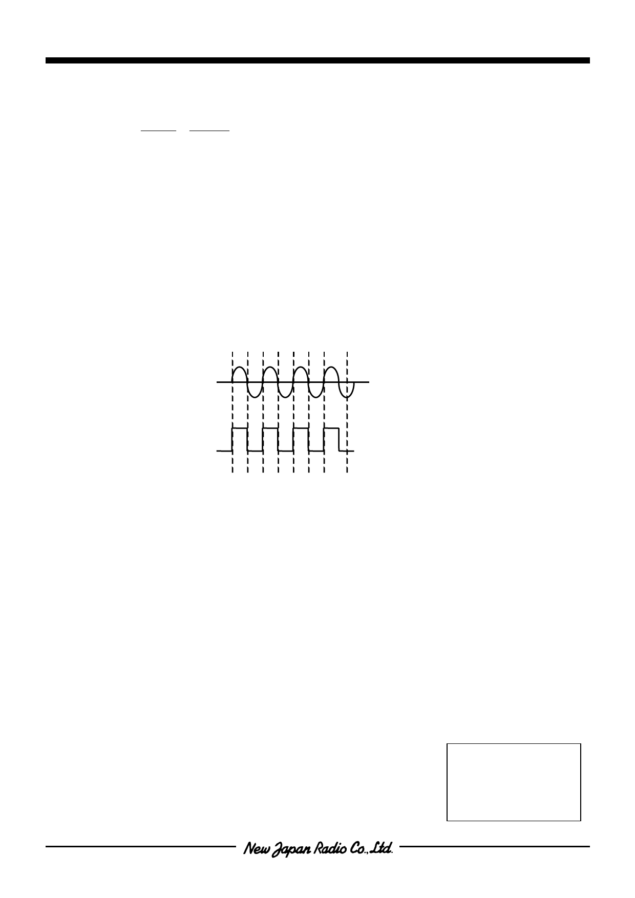
The timing chart of FG Out is as follows.
Note that the pull up resistance shall be connected to below supply voltage.
Hall input
IN+
FG Terminal voltage
[CAUTION]
The specifications on this databook are only
given for information , without any guarantee
as regards either mistakes or omissions. The
application circuits in this databook are
described only to show representative usages
of the product and not intended for the
guarantee or permission of any right including
the industrial rights.
-7 -
Share Link: 