SSM2211P 데이터 시트보기 (PDF) - Analog Devices
부품명
상세내역
제조사
SSM2211P Datasheet PDF : 16 Pages
| |||
SSM2211
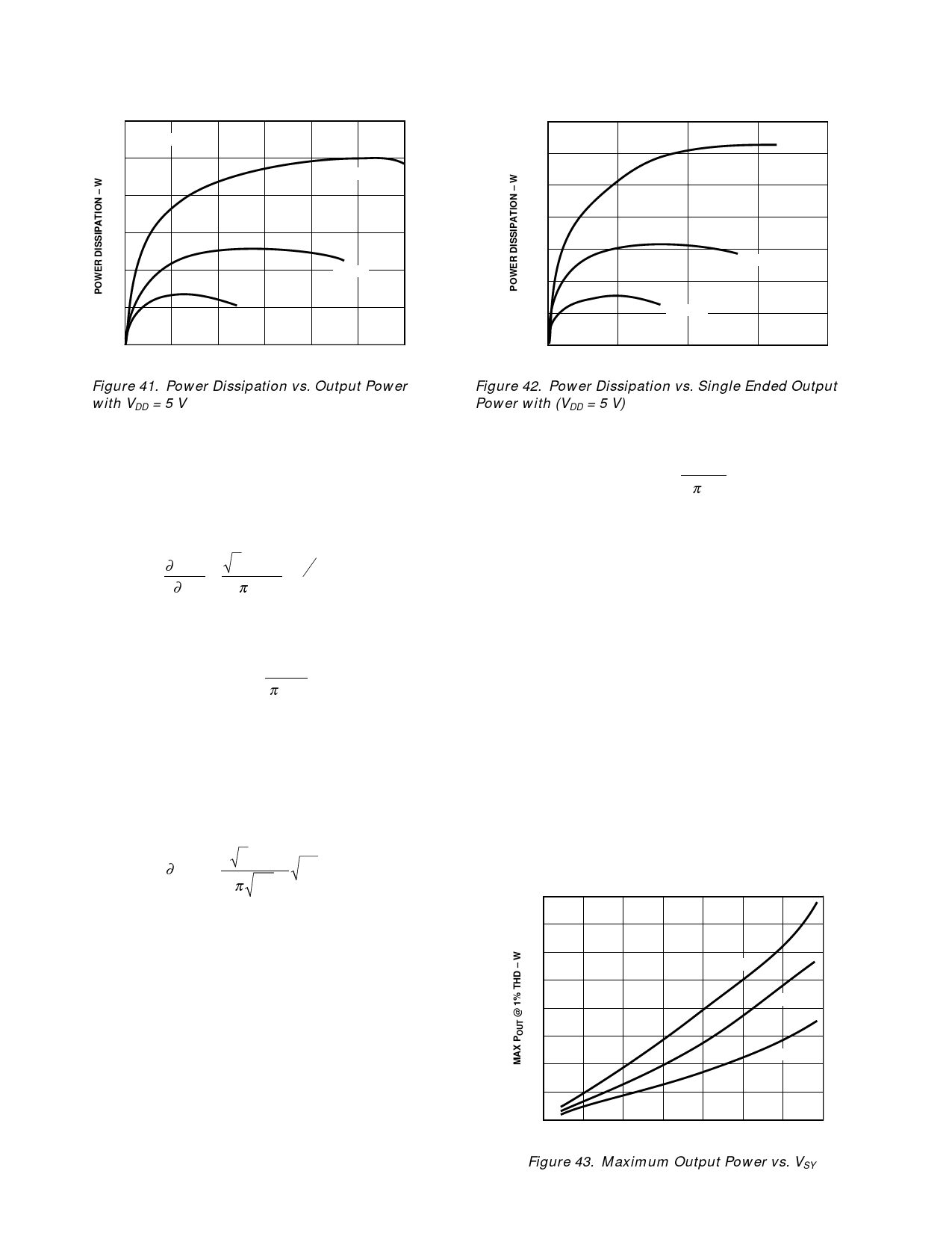
1.5
VDD = ؉5V
1.0
RL = 4⍀
0.35
0.30
VDD = ؉5V
0.25
0.20
RL = 4⍀
0.5
RL = 8⍀
RL = 16⍀
0
0
0.5
1.0
1.5
OUTPUT POWER – W
Figure 41. Power Dissipation vs. Output Power
with VDD = 5 V
Because the efficiency of a bridged output amplifier (Equation 3
divided by Equation 6) increases with the square root of PL, the
power dissipated internally by the device stays relatively flat, and
will actually decrease with higher output power. The maximum
power dissipation of the device can be found by differentiating
Equation 7 with respect to load power, and setting the derivative
equal to zero. This yields:
∂PDISS =
∂PL
2 ×VDD
πRL
−1
PL 2
−1= 0
(8)
And this occurs when:
2
PDISS ,MAX
=
2VDD
π 2RL
(9)
Using Equation 9 and the power derating curve in Figure 28,
the maximum ambient temperature can be easily found. This
insures that the SSM2211 will not exceed its maximum junction
temperature of 150°C.
The power dissipation for a single ended output application
where the load is capacitively coupled is given by:
∂PDISS = 2 2 ×VDD PL − PL
π RL
(10)
The graph of Equation 10 is shown in Figure 42.
0.15
0.10
0.05
RL = 8⍀
RL = 16⍀
0
0
0.1
0.2
0.3
0.4
OUTPUT POWER – W
Figure 42. Power Dissipation vs. Single Ended Output
Power with (VDD = 5 V)
The maximum power dissipation for a single ended output is:
2
PDISS ,MAX
=
VDD
2 π 2RL
(11)
Output Voltage Headroom
The outputs of both amplifiers in the SSM2211 can come to
within 400 mV of either supply rail while driving an 8 Ω load.
As compared to other competitors’ equivalent products, the
SSM2211 has a higher output voltage headroom. This means
that the SSM2211 can deliver an equivalent maximum output
power while running from a lower supply voltage. By running at
a lower supply voltage, the internal power dissipation of the de-
vice is reduced, as can be seen from Equation 9. This extended
output headroom, along with the Thermal Coastline package,
allows the SSM2211 to operate in higher ambient temperatures
than other competitors’ devices.
The SSM2211 is also capable of providing amplification even at
supply voltages as low as 1.7 V. Of course, the maximum power
available at the output is a function of the supply voltage.
Therefore, as the supply voltage decreases, so does the maxi-
mum power output from the device. Figure 43 shows the maxi-
mum output power versus supply voltage at various bridged-tied
load resistances. The maximum output power is defined as the
point at which the output has 1% THD.
1.6
1.4
1.2
RL = 4⍀
1.0
RL = 8⍀
0.8
0.6
RL = 16⍀
0.4
0.2
0
1.5
2.0
2.5
3.0
3.5
4.0
4.5
5.0
SUPPLY VOLTAGE – V
Figure 43. Maximum Output Power vs. VSY
–10–
REV. 0
Share Link: 