SSM2211P 데이터 시트보기 (PDF) - Analog Devices
부품명
상세내역
제조사
SSM2211P Datasheet PDF : 16 Pages
| |||
SSM2211
To find the minimum supply voltage needed to achieve a speci-
fied maximum undistorted output power, simply use Figure 43.
For example, an application requires only 500 mW to be output
for an 8 Ω speaker. With the speaker connected in a bridged out-
put configuration, the minimum supply voltage required is 3.3 V.
Shutdown Feature
The SSM2211 can be put into a low power consumption shut-
down mode by connecting Pin 1 to 5 V. In shutdown mode, the
SSM2211 has an extremely low supply current of less than 10 nA.
This makes the SSM2211 ideal for battery powered applications.
Pin 1 should be connected to ground for normal operation.
Connecting Pin 1 to VDD will mute the outputs and put the
SSM2211 into shutdown mode. A pull-up or pull-down resistor
is not required. Pin 1 should always be connected to a fixed
potential, either VDD or ground, and never be left floating. Leav-
ing Pin 1 unconnected could produce unpredictable results.
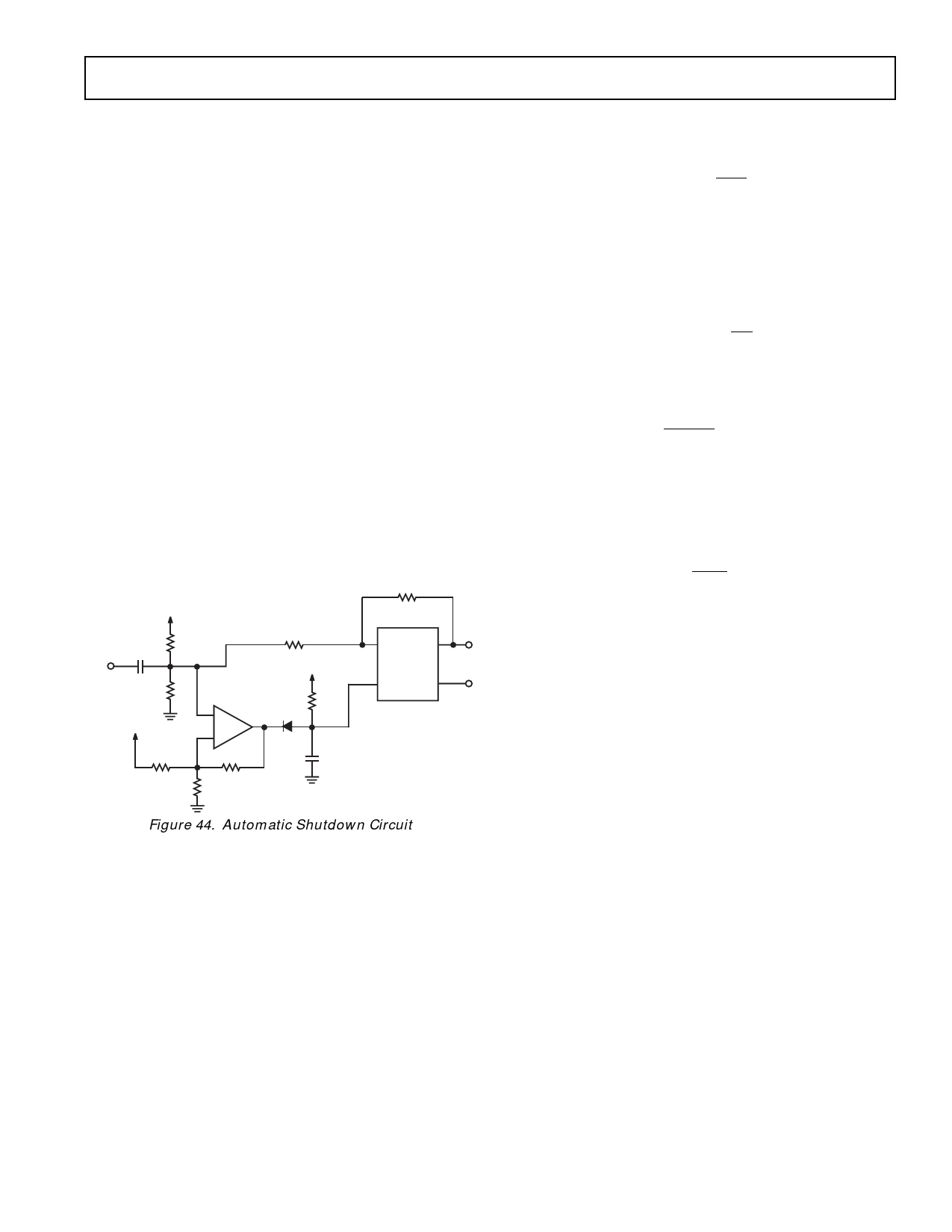
Automatic Shutdown Sensing Circuit
Figure 44 shows a circuit that can be used to automatically take
the SSM2211 in and out of shutdown mode. This circuit can be
set to turn the SSM2211 on when an input signal of a certain
amplitude is detected. The circuit will also put the SSM2211
into its low-power shutdown mode once an input signal is not
sensed within a certain amount of time. This can be useful in a
variety of portable radio applications where power conservation
is critical.
VDD
C2
VIN
VDD
R5
R6
A2
؊
؉
OP181
R1
R3
R2
R8
R7
VDD
R4
4
5
SSM2211
1
8
A1
D1
NOTE: ADDITIONAL PINS
OMITTED FOR CLARITY
C1
Figure 44. Automatic Shutdown Circuit
The input signal to the SSM2211 is also connected to the non-
inverting terminal of A2. R1, R2, and R3 set the threshold volt-
age of when the SSM2211 will be taken out of shutdown mode.
D1 half-wave rectifies the output of A2, discharging C1 to
ground when an input signal greater than the set threshold volt-
age is detected. R4 controls the charge time of C1, which sets
the time until the SSM2211 is put back into shutdown mode af-
ter the input signal is no longer detected.
R5 and R6 are used to establish a voltage reference point equal
to half of the supply voltage. R7 and R8 set the gain of the
SSM2211. D1 should be a 1N914 or equivalent diode and A2
should be a rail-to-rail output amplifier, such as an OP181 or
equivalent. This will ensure that C1 will discharge sufficiently to
bring the SSM2211 out of shutdown mode.
To find the appropriate component values, first the gain of A2
must be determined by:
AV ,
MIN
= VSY
VTHS
(12)
Where, VSY is the single supply voltage and,
VTHS is the threshold voltage.
AV should be set to a minimum of 2 for the circuit to work prop-
erly. Next choose R1 and set R2 to:
R2
=
R11−
2
AV
(13)
Find R3 as:
( ) R3 = R1× R2
R1+ R2
AV −1
(14)
C1 can be arbitrarily set, but should be small enough to not cause
A2 to become capacitively overloaded. R4 and C1 will control the
shutdown rate. To prevent intermittent shutdown with low
frequency input signals, the minimum time constant should be:
R4 × C1 ≥ 10
fLOW
(15)
Where, fLOW is the lowest input frequency expected.
Shutdown Circuit Design Example
In this example a portable radio application requires the
SSM2211 to be turned on when an input signal greater than
50 mV is detected. The device should return to shutdown mode
within 500 ms after the input signal is no longer detected. The
lowest frequency of interest is 200 Hz, and a +5 V supply is
being used.
The minimum gain of the shutdown circuit from Equation 12 is
AV = 100. R1 is set to 100 kΩ, and using Equation 13 and
Equation 14, R2 = 98 kΩ and R3 = 4.9 MΩ. C1 is set to
0.01 µF, and based on Equation 15, R4 is set to 10 MΩ. To
minimize power supply current, R5 and R6 are set to 10 MΩ.
The above procedure will provide an adequate starting point for
the shutdown circuit. Some component values may need to be
adjusted empirically to optimize performance.
Turn On Popping Noise
During power-up or release from shutdown mode, the midrail
bypass capacitor, CB, determines the rate at which the
SSM2211 starts up. By adjusting the charging time constant of
CB, the start-up pop noise can be pushed into the sub-audible
range, greatly reducing startup popping noise. On power-up, the
midrail bypass capacitor is charged through an effective resis-
tance of 25 kΩ. To minimize start-up popping, the charging
time constant for CB should be greater than the charging time
constant for the input coupling capacitor, CC.
CB × 25 kΩ > CC RI
(16)
REV. 0
–11–
Share Link: 