NVD0.1CKK-M6 데이터 시트보기 (PDF) - Power-One Inc.
부품명
상세내역
제조사
NVD0.1CKK-M6 Datasheet PDF : 11 Pages
| |||
NV Series: 4 - 6W DC/DC Converters
9-36V, 18-36V, 36-72V & 16-75V Inputs
3.3V, 5.0V, 12V, 15V, ±5.0V, ±12V, ±15V & ±24V Outputs
Product Specifications
Oct 2001
Output Specifications
All specifications apply over input voltage, output load and temperature range, unless otherwise noted.
All Models
Parameter
Output Voltage Accuracy
Conditions/Description
Vin.Nom, 50% Io.Max
Min Nom Max
±1
Units
%Vo
Line Regulation
Load Regulation
Vin.Min to Vin.Max, 50% Io.Max
Vin.Nom, Io.Min to Io.Max
3.3Vo
Other Output Voltages
±1
±3.5
±3.0
%Vo
%Vo
%Vo
Maximum Output Capacitance
Total, for single and dual outputs
3.3Vo
5Vo, ±5Vo
12Vo, ±12Vo
15Vo, ±12Vo
±24Vo
680
µF
680
µF
150
µF
100
µF
45
µF
Dynamic Regulation
Peak Deviation
50-100% Io.Max load step
change
5.0
%Vo
Settling Time
Output Voltage Ripple
to 1% error band
Vin.Min to Vin.Max, Io.Min to Io
Max, 20MHz Bandwidth
3.3Vo
1.0
ms
50
80
mVp-p
5Vo, ±5Vo
12Vo, ±12Vo, ±24Vo
50
80
mVp-p
0.8
1
%Vo p-p
Output Current Limit Threshold
Switching Frequency
Output Current Limit Threshold
Vin.Nom, Io.Max
120
250
200 %Io.Max
KHz
Temperature Coefficient
0.02 %Vo/°C
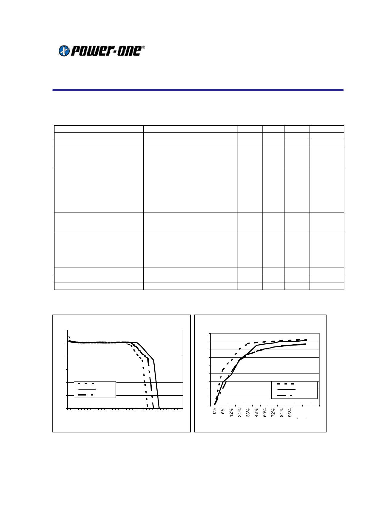
Typical characteristic curves for single 5V output type
Vout (V)
6.00
Output Voltage Vs Load
5.00
4.00
3.00
2.00
Vin Min
Vin Nom
1.00
Vin Max
0.00
25% 50% 75% 100%
Iout (A)
Efficiency
90%
80%
70%
60%
50%
40%
30%
20%
10%
0%
Efficiency Vs Load
Vin Min
Vin Nom
Vin Max
Iout (A)
18-Oct-01
Rev 1.0
www.power-one.com
Page 4 of 11
Share Link: 