DDU7F-100M 데이터 시트보기 (PDF) - Data Delay Devices
부품명
상세내역
제조사
DDU7F-100M Datasheet PDF : 4 Pages
| |||
10-TAP, TTL-INTERFACED
FIXED DELAY LINE
(SERIES DDU7F)
DDU7F
data
delay
3
®
devices, inc.
FEATURES
• Ten equally spaced outputs
• Fits standard 14-pin DIP socket
• Low profile
• Auto-insertable
• Input & outputs fully TTL interfaced & buffered
• 10 T2L fan-out capability
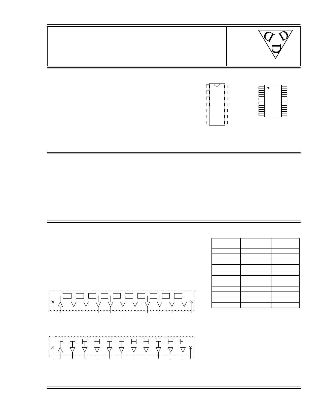
PACKAGES
IN 1 14 VCC
N/C 2 13 T1
T2 3 12 T3
T4 4 11 T5
T6 5 10 T7
T8 6 9 T9
GND 7 8 T10
IN 1
T2 2
T4 3
T6 4
T8 5
T10 6
N/C 7
GND 8
16 VCC
15 T1
14 T3
13 T5
12 T7
11 T9
10 N/C
9 N/C
DDU7F-xx DIP
DDU7F-xxA2 Gull-Wing
DDU7F-xxB2 J-Lead
DDU7F-xxM Military DIP
Military SMD
DDU7F-xxMC3
FUNCTIONAL DESCRIPTION
PIN DESCRIPTIONS
The DDU7F-series device is a 10-tap digitally buffered delay line. The
IN Signal Input
signal input (IN) is reproduced at the outputs (T1-T10), shifted in time by an T1-T10 Tap Outputs
amount determined by the device dash number. The nominal tap-to-tap
VCC +5 Volts
delay increment is given by 1/10 of the dash number. For dash numbers
GND Ground
less than 50, the total delay of the line is measured from T1 to T10, with the
nominal value given by 9 times the increment. The inherent delay from IN to T1 is nominally 3.5ns. For
dash numbers greater than or equal to 50, the total delay of the line is measured from IN to T10, with the
nominal value given by the dash number.
SERIES SPECIFICATIONS
• Minimum input pulse width: 20% of total delay
• Output rise time: 2ns typical
• Supply voltage: 5VDC ± 5%
• Supply current: ICCL = 50ma typical
ICCH = 15ma typical
• Operating temperature: 0° to 70° C
• Temp. coefficient of total delay: 100 PPM/°C
3.5ns 10% 10% 10% 10% 10% 10% 10% 10% 10%
VCC IN T1 T2 T3 T4 T5 T6 T7 T8 T9 T10 GND
Functional diagram for dash numbers < 50
10% 10% 10% 10% 10% 10% 10% 10% 10% 10%
DASH NUMBER SPEC.’S
Part
Number
DDU7F-10
DDU7F-20
DDU7F-25
DDU7F-50
DDU7F-100
DDU7F-150
DDU7F-200
DDU7F-250
DDU7F-300
DDU7F-400
DDU7F-500
Total
Delay (ns)
9 ± 2.0 *
18 ± 2.0 *
22.5 ± 2.0 *
50 ± 2.5
100 ± 5.0
150 ± 7.5
200 ± 10.0
250 ± 12.5
300 ± 15.0
400 ± 20.0
500 ± 25.0
Delay Per
Tap (ns)
1.0 ± 0.5
2.0 ± 1.0
2.5 ± 1.0
5.0 ± 2.0
10.0 ± 3.0
15.0 ± 3.0
20.0 ± 3.0
25.0 ± 3.0
30.0 ± 3.0
40.0 ± 4.0
50.0 ± 5.0
* Total delay is referenced to first tap
Input to first tap = 3.5ns ± 1ns
NOTE: Any dash number between 10 and
500 not shown is also available.
VCC IN T1 T2 T3 T4 T5 T6 T7 T8 T9 T10 GND
Functional diagram for dash numbers >= 50
©1997 Data Delay Devices
Doc #97016
DATA DELAY DEVICES, INC.
1
1/29/97
3 Mt. Prospect Ave. Clifton, NJ 07013
Powered by ICminer.com Electronic-Library Service CopyRight 2003
Share Link: 