P90CE201 데이터 시트보기 (PDF) - Philips Electronics
부품명
상세내역
제조사
P90CE201 Datasheet PDF : 77 Pages
| |||
Philips Semiconductors
16-bit microcontroller
Product specification
P90CE201
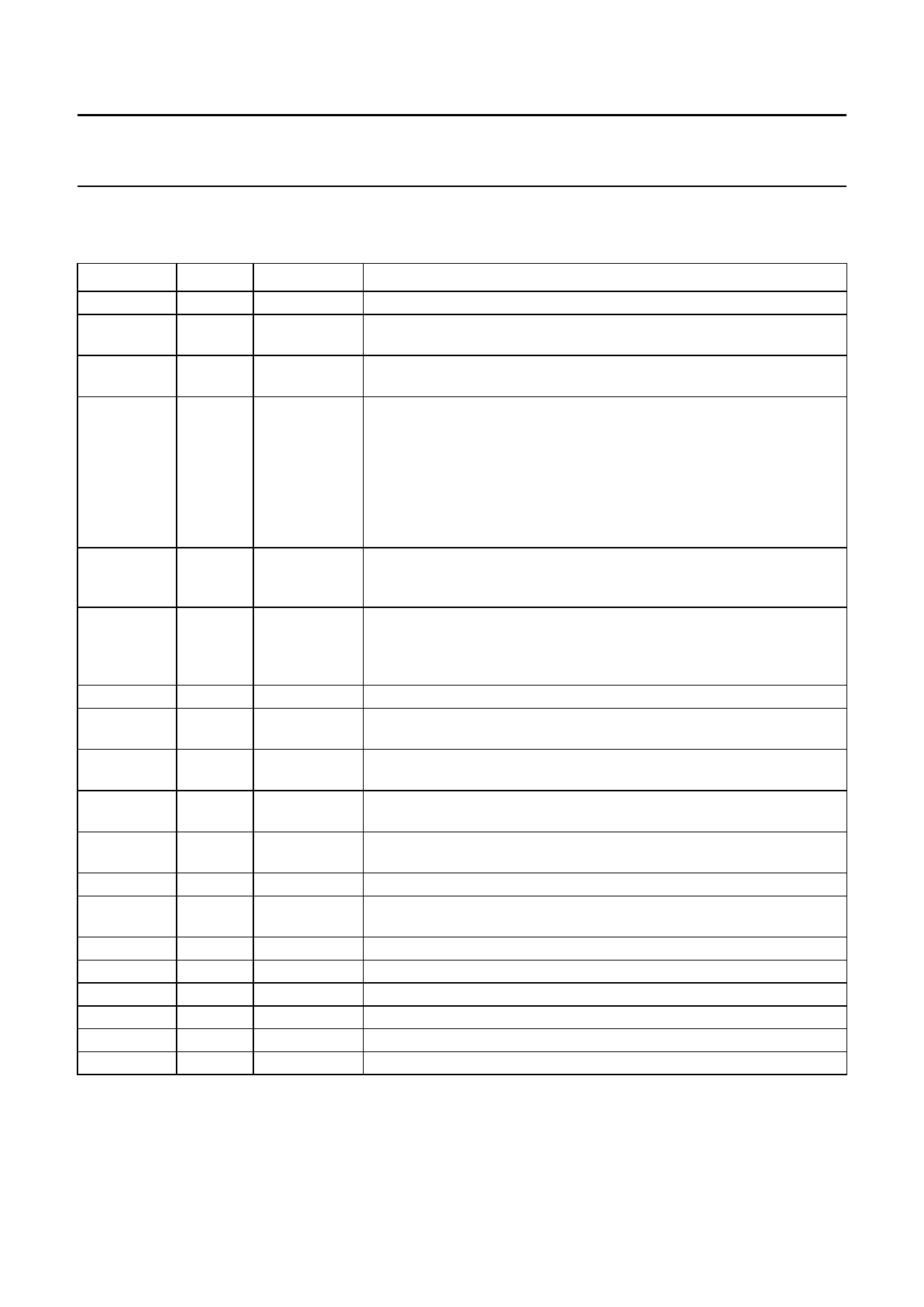
4.2 Pin description
Table 1 QFP64 package.
MNEMONIC
RXD
SDA2
SCL2
GP7/SDA1
GP6/SCL1
GP0
GP1
GP2
GP3
GP4
GP5/T1
A23/AP7
to
A16/AP0
A15 to A0
XTAL2
XTAL1
VDD1
VSS1
R/WN
CSROMN
D0 to D7
CSRAMN
VSS2
VDD2
RESET
T0
T2
TYPE
I/O
I/O
PIN NO.
1
2
I/O 3
I/O 4
5
6
7
8
9
10
11
I/O 12 to 15, 21,
22, 24, 23
FUNCTION
Receive Data. RXD is the data input for the UART interface.
Serial Data 2 (open drain). SDA2 is the data signal for the second
I2C-bus serial interface.
Serial Clock 2 (open drain). SCL2 is the clock signal for the second
I2C-bus serial interface.
General Purpose Port (active HIGH, 3-state). The alternative functions
are as follows. SCL1 is the clock signal for the first I2C-bus serial
interface. SDA1 is the data signal for the first I2C-bus serial interface.
T1 is the input pin for Timer 1.
Address Bus. Upper 8-bits of the address bus (A23 to A16). The unused
address bits can be selected as a quasi-bidirectional port (AP).
O
25, 26, 28, 27, Address Bus. Lower 16-bits of the address bus.
34, 38, 32, 30,
29, 31, 33, 35,
37, 39, 40, 42
O
16
Oscillator output. Not connected if an external clock generator is used.
I
17
Oscillator input. XTAL1 can also be used as an external clock input if
an external clock generator is used.
−
18
Supply voltage. For internal logic, address bus, data bus, RWN,
CSRAMN, CSROMN, XTAL1 and XTAL2.
−
19
Ground. For internal logic, address bus, data bus, RWN, CSRAMN,
CSROMN, XTAL1 and XTAL2.
O
20
Read (active HIGH)/Write (active LOW). This controls the direction of
data flow.
O
36
Chip Select ROM (active LOW). This signal selects external ROM.
O
44, 46, 48, 49, Data Bus. 8-bit data bus.
47, 45, 43, 41
O
50
Chip Select RAM (active LOW). This signal enables external RAM.
−
51
Ground. For all other periphery pins (quiet port).
−
52
Supply voltage. For all other periphery pins (quiet port).
I
53
Reset (active HIGH). Input pin for an external reset.
I
54
Timer 0. Input pin for cycle and event counting using Timer 0.
I
55
Timer 2. Input pin for cycle and event counting using Timer 2.
August 1993
6
Share Link: 