P89LPC980FDH 데이터 시트보기 (PDF) - NXP Semiconductors.
부품명
상세내역
제조사
P89LPC980FDH
NXP Semiconductors.

P89LPC980FDH Datasheet PDF : 85 Pages
| |||
NXP Semiconductors
P89LPC980/982/983/985
8-bit microcontroller with accelerated two-clock 80C51 core
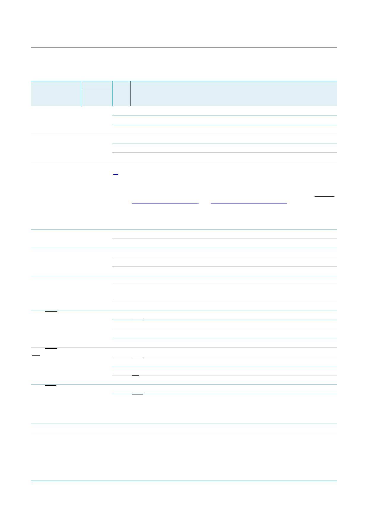
Table 3. Pin description …continued
Symbol
Pin
Type Description
PLCC28,
TSSOP28
P0.6/CMP1/KBI6 20
I/O P0.6 — Port 0 bit 6. High current source.
O CMP1 — Comparator 1 output.
I
KBI6 — Keyboard input 6.
P0.7/KBI7/T1
19
I/O P0.7 — Port 0 bit 7. High current source.
I/O T1 — Timer/counter 1 external count input or overflow output.
I
KBI7 — Keyboard input 7.
P1.0 to P1.7
I/O, I
[1]
Port 1: Port 1 is an 8-bit I/O port with a user-configurable output type, except for
three pins as noted below. During reset Port 1 latches are configured in the input
only mode with the internal pull-up disabled. The operation of the configurable
Port 1 pins as inputs and outputs depends upon the port configuration selected.
Each of the configurable port pins are programmed independently. Refer to Section
7.16.1 “Port configurations” and Table 13 “Static characteristics” for details. P1.2 to
P1.3 are open drain when used as outputs. P1.5 is input only.
All pins have Schmitt trigger inputs.
Port 1 also provides various special functions as described below:
P1.0/TXD
18
I/O P1.0 — Port 1 bit 0.
O TXD — Transmitter output for serial port.
P1.1/RXD/T2EX 17
I/O P1.1 — Port 1 bit 1.
I
RXD — Receiver input for serial port.
I
T2EX — Timer/counter 2 external capture input.
P1.2/SCL/T0
12
I/O P1.2 — Port 1 bit 2 (open-drain when used as output).
I/O T0 — Timer/counter 0 external count input or overflow output (open-drain when
used as output).
I/O SCL — I2C-bus serial clock input/output.
P1.3/INT0/SDA/ 11
T4
I/O P1.3 — Port 1 bit 3 (open-drain when used as output).
I
INT0 — External interrupt 0 input.
I/O SDA — I2C-bus serial data input/output.
I/O T4 — Timer/counter 4 external count input or overflow output.
P1.4/INT1/T4EX/ 10
SS
I/O P1.4 — Port 1 bit 4. High current source.
I
INT1 — External interrupt 1 input.
I
T4EX — Timer/counter 4 external capture input.
I
SS — SPI Slave select. (pin remap)
P1.5/RST
6
I
P1.5 — Port 1 bit 5 (input only).
I
RST — External Reset input during power-on or if selected via UCFG1. When
functioning as a reset input, a LOW on this pin resets the microcontroller, causing
I/O ports and peripherals to take on their default states, and the processor begins
execution at address 0. Also used during a power-on sequence to force ISP mode.
P1.6/MISO
5
I/O P1.6 — Port 1 bit 6. High current source.
I/O MISO — SPI master in slave out. When configured as master, this pin is input,
when configured as slave, this pin is output. (pin remap)
P89LPC980_982_983_985
Product data sheet
Rev. 4 — 15 June 2010
© NXP B.V. 2010. All rights reserved.
11 of 85
Share Link: