CXD1179Q 데이터 시트보기 (PDF) - Sony Semiconductor
부품명
상세내역
제조사
CXD1179Q Datasheet PDF : 14 Pages
| |||
Pin No. Symbol
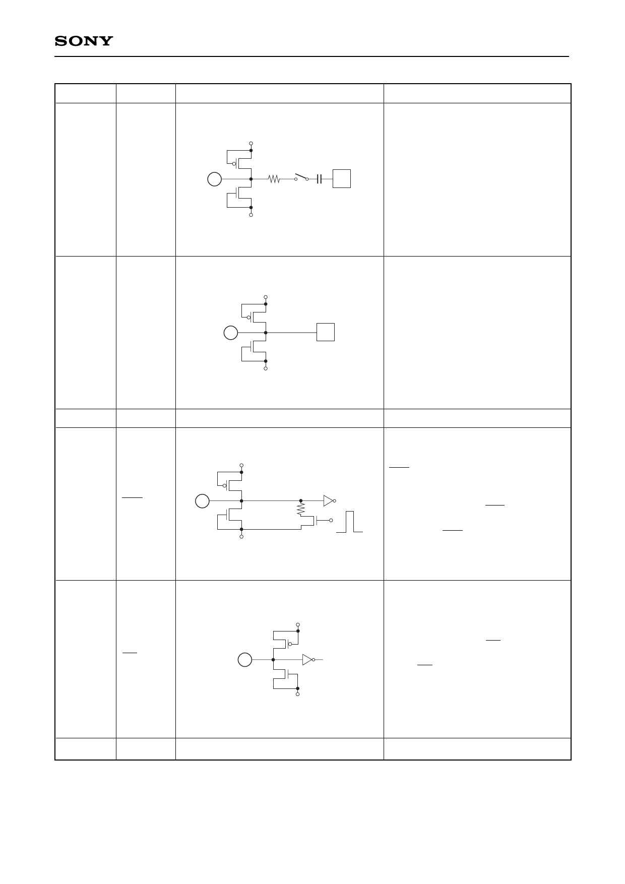
26
VREF
Equivalent circuit
AVDD
26
AVSS
CXD1179Q
Description
Clamp reference voltage input.
Clamps so that the reference voltage
and the input signal during clamp
interval are equal.
27
CCP
28, 31 DVSS
29
CLE
AVDD
27
AVSS
DVDD
29
DVSS
Integrates the clamp control voltage.
The relationship between the changes
in CCP voltage and in VIN voltage is
positive phase.
Digital ground
CLAMP
PULSE
The clamp function is enabled when
CLE = Low.
The clamp function is set to off and
the converter functions as a normal
A/D converter when CLE = High.
The clamp pulse can be measured by
connecting CLE to DVDD through a
several hundred Ω resistor.
30
OE
32
NC
DVDD
30
DVSS
—5—
Data is output when OE = Low.
Pins D0 to D7 are at high impedance
when OE = High.
NC pin
Share Link: 