CXD1179Q 데이터 시트보기 (PDF) - Sony Semiconductor
부품명
상세내역
제조사
CXD1179Q Datasheet PDF : 14 Pages
| |||
CXD1179Q
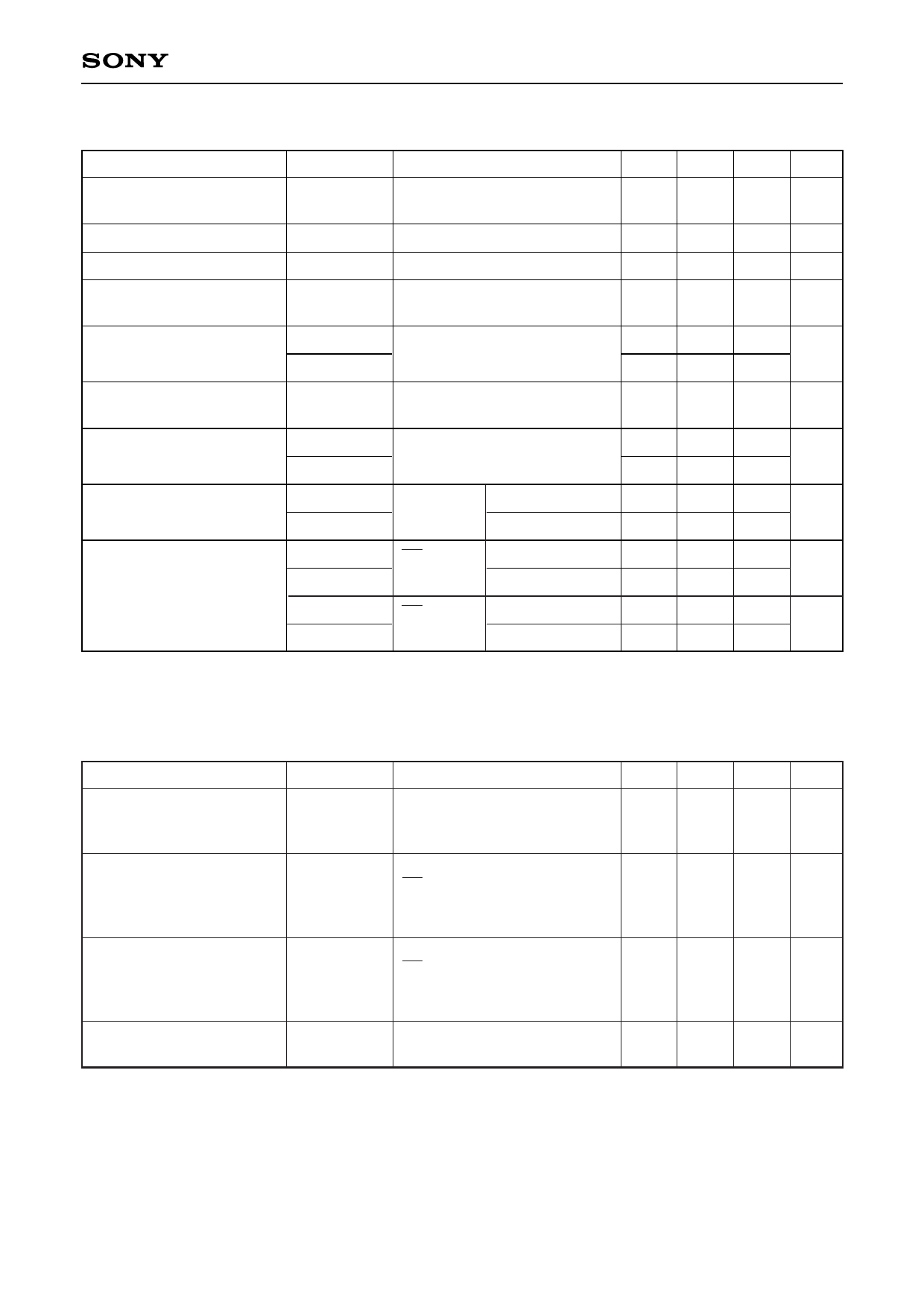
DC characteristics
Item
Supply current
Reference pin current
Analog input capacitance
Reference resistance
(VRT to VRB)
Self-bias I
Self-bias II
Digital input voltage
Digital input current
Digital output current
Symbol
IDD
IREF
CIN
RREF
VRB1
VRT1 – VRB1
VRT2
VIH
VIL
IIH
IIL
IOH
IOL
IOZH
IOZL
(Fc = 35MSPS, VDD = 5 V, VRB = 0.5 V, VRT = 2.5 V, Ta = 25 °C)
Conditions
Fc = 35MSPS
NTSC ramp wave input
VIN = 1.5 V + 0.07 Vrms
Min. Typ. Max. Unit
16 22 mA
4.5 6.1 8.7 mA
8
pF
230 330 440 Ω
Shorts VRB and VRBS
Shorts VRT and VRTS
0.52 0.56 0.60
V
1.96 2.10 2.24
VRB = AGND
Shorts VRT and VRTS
2.13 2.33 2.53 V
VDD = 4.75 to 5.25 V
Ta = –40 to +85 °C
3.5
V
0.5
VDD = max
VIH = VDD
VIL = 0 V
5
µA
5
OE = VSS
VDD = min
VOH = VDD – 0.5 V –1.1
VOL = 0.4 V
3.7
–2.5
6.5
mA
OE = VDD
VDD = max
VOH = VDD
VOL = 0 V
16
µA
16
Timing
(Fc = 35MSPS, VDD = 5 V, VRB = 0.5 V, VRT = 2.5 V, Ta = 25 °C)
Item
Symbol
Conditions
Min. Typ. Max. Unit
Output data delay
TDL
With TTL 1 gate and 10 pF load
VDD = 4.75 to 5.25 V
7
Ta = –40 to +85 °C
13 18 ns
Tri-state output
enable time
RL = 1 kΩ, CL = 15 pF
tPZH
OE = 5 V → 0 V
tPZL
VDD = 4.75 to 5.25 V
Ta = –40 to +85 °C
5
8
14 ns
Tri-state output
disable time
RL = 1 kΩ, CL = 15 pF
tPHZ
OE = 0V → 5 V
tPLZ
VDD = 4.75 to 5.25 V
Ta = –40 to +85 °C
4
6.5 11 ns
Clamp pulse width∗1
tcpw
Fc = 14MSPS, CIN = 10 µF
for NTSC wave
1.75 2.75 3.75 µs
∗1 The clamp pulse width is for NTSC as an example. Adjust the rate to the clamp pulse cycle (1/15.75 kHz
for NTSC) for other processing systems to equal the values for NTSC.
—8—
Share Link: 