PCD5013 데이터 시트보기 (PDF) - Philips Electronics
부품명
상세내역
제조사
PCD5013 Datasheet PDF : 76 Pages
| |||
Philips Semiconductors
FLEX™ roaming decoder II
Product specification
PCD5013
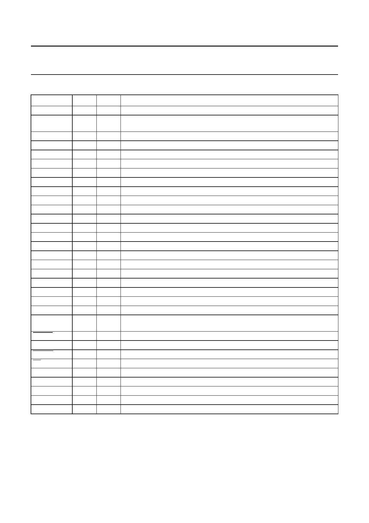
7 PINNING
SYMBOL
PIN
I/O
DESCRIPTION
TOUT0
1
O 3-state test output; note 1
OSCPD
VDD1
TEST2
XTAL
2
I internal oscillator power-down; connected to VSS when using the internal oscillator,
connected to VDD when using an external source
3
− supply voltage
4
I manufacturing test mode input pin; has to be connected to VSS
5
O 76.8 or 160 kHz crystal oscillator output
EXTAL
6
I 76.8 or 160 kHz crystal oscillator input or external clock input
VSS1
TEST3
TOUT3
7
− ground supply
8
I manufacturing test mode input pin; has to be connected to VSS
9
O 3-state test output; note 1
LOBAT
10
I low battery voltage detect input
EXTS1
11
I most significant bit (MSB) of the symbol currently being decoded
EXTS0
12
I least significant bit (LSB) of the symbol currently being decoded
VDD2
SYMCLK
13
− supply voltage
14
O recovered symbol clock output
S7
15
O receiver control output port, 3-state
S6
16
O receiver control output port, 3-state
TOUT2
17
O 3-state test output; note 1
S5
18
O receiver control output port, 3-state
S4
19
O receiver control output port, 3-state
S3
20
O receiver control output port, 3-state
S2
21
O receiver control output port, 3-state
S1
22
O receiver control output port, 3-state
S0/IFIN
23
I/O receiver control output port, 3-state when using external demodulator; limited
IF input 455 or 140 kHz when using internal demodulator
RESET
24
I active LOW reset input
TOUT1
25
O 3-state test output; note 1
READY
26
O output driven LOW when the PCD5013 is ready for an SPI packet
SS
27
I slave select input for SPI communications
SCK
28
I serial clock input for SPI communications
VSS2
MOSI
29
− ground supply
30
I data input for SPI communications
MISO
31
O data output for SPI communications, 3-state
CLKOUT
32
O 38.4 kHz clock output (derived from 76.8 kHz oscillator); note 2
Notes
1. These test outputs may be either left unconnected or connected to VSS in the application.
2. For a 160 kHz oscillator either a 38.4 or a 40 kHz output frequency can be selected. See Section 8.4.4.
1999 Apr 12
5
Share Link: 