PCF2103 데이터 시트보기 (PDF) - Philips Electronics
부품명
상세내역
제조사
PCF2103 Datasheet PDF : 56 Pages
| |||
Philips Semiconductors
LCD controllers/drivers
Product specification
PCF2103 family
7.8 Address Counter (AC)
The address counter assigns addresses to the DDRAM
and CGRAM for reading and writing and is set by the
commands ‘set CGRAM address’ and ‘set DDRAM
address’. After a read/write operation the address counter
is automatically incremented or decremented by 1.
The address counter contents are output to the bus
(DB6 to DB0) when RS = 0 and R/W = 1.
7.9 Display Data RAM (DDRAM)
The DDRAM stores up to 80 characters of display data
represented by 8-bit character codes. RAM locations
which are not used for storing display data can be used as
general purpose RAM. The basic RAM-to-display
addressing scheme is shown in Fig.2. With no display shift
the characters represented by the codes in the first
24 RAM locations starting at address 00 in line 1 are
displayed. Figures 3 and 4 show the display mapping for
right and left shift respectively.
When data is written to or read from the DDRAM
wrap-around occurs from the end of one line to the start of
the next line. When the display is shifted each line wraps
around within itself, independently of the others. Thus all
lines are shifted and wrapped around together.
The address ranges and wrap-around operations for the
various modes are shown in Table 4.
7.10 Character Generator ROM (CGROM)
The Character Generator ROM (CGROM) generates
240 character patterns in 5 × 8 dot format from 8-bit
character codes. Figure 6 shows the character set that is
currently implemented.
7.11 Character Generator RAM (CGRAM)
Up to 16 user defined characters may be stored in the
CGRAM. Some CGRAM characters (see Fig.14) are also
used to drive icons (6 if icons blink and both icon rows are
used in application; 3 if no blink but both icon rows are
used in application; 0 if no icons are driven by the icon
rows). The CGROM and CGRAM use a common address
space, of which the first column is reserved for the
CGRAM (see Fig.6). Figure 7 shows the addressing
principle for the CGRAM.
7.12 Cursor control circuit
The cursor control circuit generates the cursor (underline
and/or cursor blink as shown in Fig.5) at the DDRAM
address contained in the address counter. When the
address counter contains the CGRAM address the cursor
will be inhibited.
7.13 Timing generator
The timing generator produces the various signals
required to drive the internal circuitry. Internal chip
operation is not disturbed by operations on the data buses.
7.14 LCD row and column drivers
The PCF2103 contains 18 row and 60 column drivers,
which connect the appropriate LCD bias voltages in
sequence to the display in accordance with the data to be
displayed. R17 and R18 drive the icon rows.
The bias voltages and the timing are selected
automatically when the number of lines in the display is
selected. Figures 8, 9 and 10 show typical waveforms.
Unused outputs should be left unconnected.
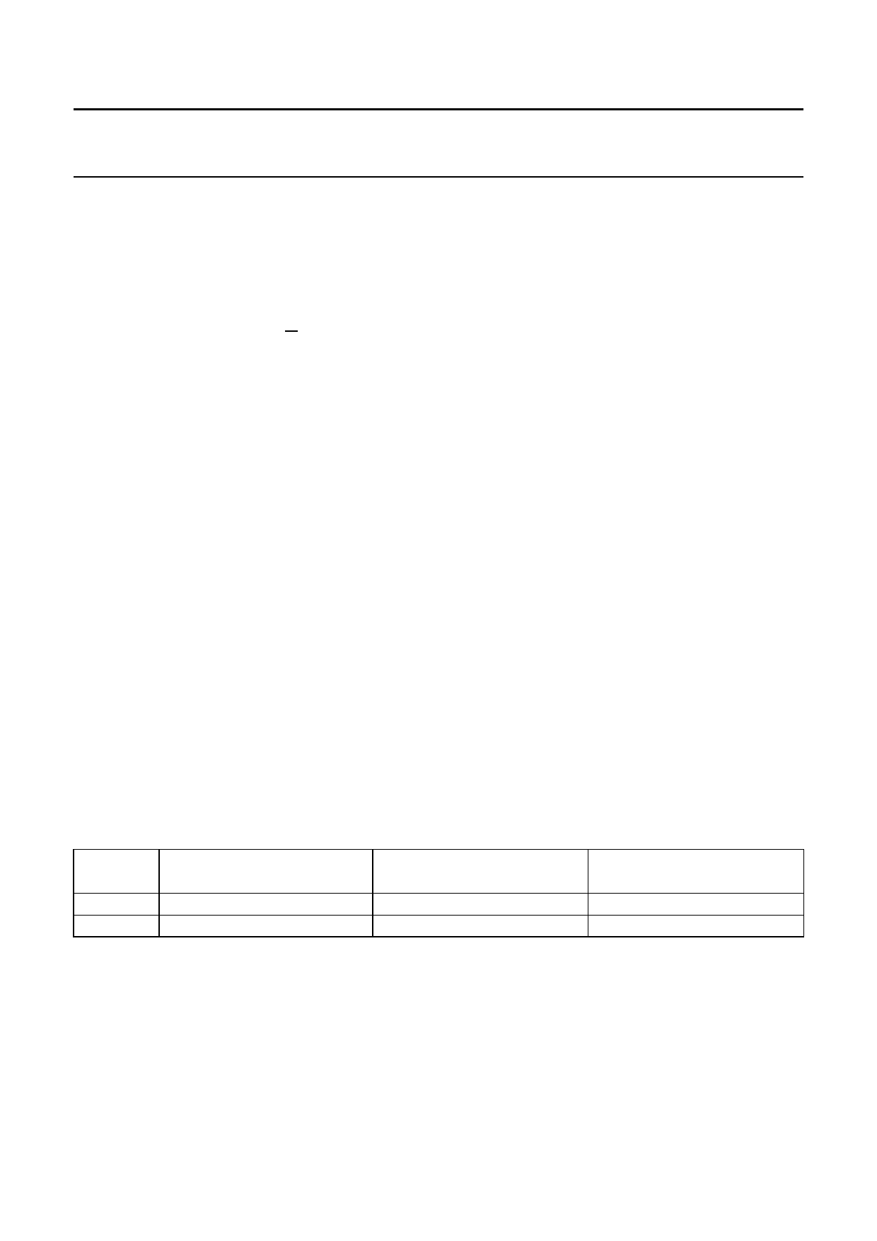
Table 4 Address space and wrap-around operation
MODE
1 × 24
2 × 12
ADDRESS SPACE
00H to 4FH
00H to 27H; 40H to 67H
READ/WRITE
WRAP-AROUND(1)
4FH to 00H
27H to 40H; 67H to 00H
Notes
1. Moves to next line.
2. Stays within line.
DISPLAY SHIFT
WRAP-AROUND(2)
4FH to 00H
27H to 00H; 67H to 40H
1998 May 11
8
Share Link: 