HT48RA0A 데이터 시트보기 (PDF) - Holtek Semiconductor
부품명
상세내역
제조사
HT48RA0A Datasheet PDF : 31 Pages
| |||
HT48RA0A
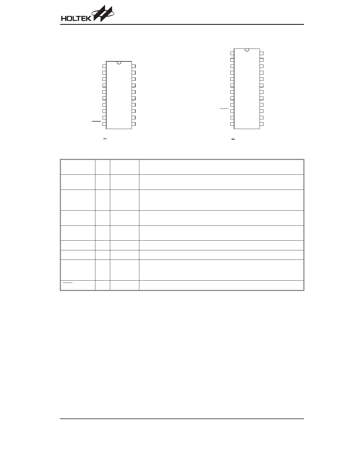
Pin Assignment
PA1 1
PA0 2
PB1 3
PB0 4
P C 0 /R E M
5
VDD 6
O SC2 7
O SC1 8
VSS 9
R E S 10
20 P A 2
19 P A 3
18 P A 4
17 P A 5
16 P A 6
15 P A 7
14 P B 2
13 P B 3
12 P B 4
11 P B 5
H T48R A 0A
2 0 S O P -A
PA1 1
PA0 2
PB1 3
PB0 4
P C 0 /R E M 5
VDD 6
O SC2 7
O SC1 8
VSS 9
R E S 10
N C 11
N C 12
24 P A 2
23 P A 3
22 P A 4
21 P A 5
20 P A 6
19 P A 7
18 P B 2
17 P B 3
16 P B 4
15 P B 5
14 P B 6
13 P B 7
H T48R A 0A
2 4 S O P -A
Pin Description
Pin Name
PA0~PA7
PB0, PB1
PB2~PB7
PC0/REM
VDD
VSS
OSC2
OSC1
RES
I/O
Code
Option
Description
I/O
¾
Bidirectional 8-bit input/output port with pull-high resistors. Each bit can be de-
termined as NMOS output or Schmitt trigger input by software instructions.
I/O
Wake-up
or None
2-bit bidirectional input/output lines with pull-high resistors. Each bit can be de-
termined as NMOS output or Schmitt trigger input by software instructions.
Each bit can also be configured as wake-up input by code option.
I
Wake-up or 6-bit Schmitt trigger input lines with pull-high resistors. Each bit can be config-
None ured as a wake-up input by code option.
O
Level or Level or carrier output pin
Carrier PC0 can be set as CMOS output pin or carrier output pin by code option.
¾
¾
Positive power supply
¾
¾
Negative power supply, ground
I
O
Crystal
or RC
OSC1, OSC2 are connected to an RC network or a crystal (determined by
code option) for the internal system clock. In the case of RC operation, OSC2
is the output terminal for 1/4 system clock (NMOS open drain output).
I
¾
Schmitt trigger reset input. Active low.
Absolute Maximum Ratings
Supply Voltage ...........................VSS-0.3V to VSS+4.0V
Input Voltage..............................VSS-0.3V to VDD+0.3V
Storage Temperature ............................-50°C to 125°C
Operating Temperature...........................-40°C to 85°C
Note: These are stress ratings only. Stresses exceeding the range specified under ²Absolute Maximum Ratings² may
cause substantial damage to the device. Functional operation of this device at other conditions beyond those
listed in the specification is not implied and prolonged exposure to extreme conditions may affect device reliabil-
ity.
Rev. 1.70
2
July 16, 2003
Share Link: 