PEMB9 데이터 시트보기 (PDF) - NXP Semiconductors.
부품명
상세내역
제조사
PEMB9 Datasheet PDF : 8 Pages
| |||
NXP Semiconductors
PNP/PNP resistor-equipped transistors;
R1 = 10 kΩ, R2 = 47 kΩ
Product data sheet
PEMB9; PUMB9
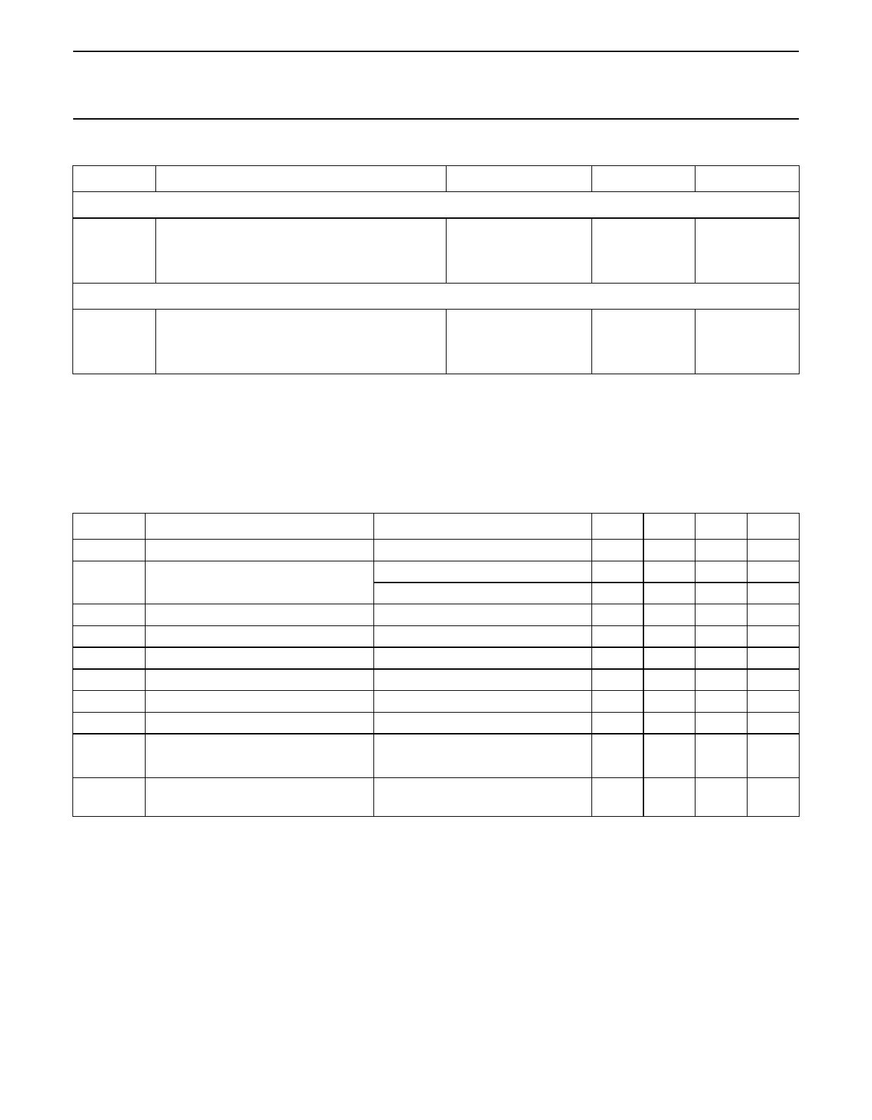
THERMAL CHARACTERISTICS
SYMBOL
PARAMETER
Per transistor
Rth j-a
thermal resistance from junction to ambient
SOT363
SOT666
Per device
Rth j-a
thermal resistance from junction to ambient
SOT363
SOT666
CONDITIONS
Tamb ≤ 25 °C
note 1
notes 1 and 2
Tamb ≤ 25 °C
note 1
note 1
VALUE
625
625
416
416
Notes
1. Device mounted on an FR4 printed-circuit board, single-sided copper, standard footprint.
2. Reflow soldering is the only recommended soldering method.
UNIT
K/W
K/W
K/W
K/W
CHARACTERISTICS
Tamb = 25 °C unless otherwise specified.
SYMBOL
PARAMETER
ICBO
collector-base cut-off current
ICEO
collector-emitter cut-off current
IEBO
hFE
VCEsat
Vi(off)
Vi(on)
R1
R-----2--
R1
Cc
emitter-base cut-off current
DC current gain
saturation voltage
input-off voltage
input-on voltage
input resistor
resistor ratio
collector capacitance
CONDITIONS
VCB = −50 V; IE = 0
VCE = −30 V; IB = 0
VCE = −30 V; IB = 0; Tj = 150 °C
VEB = −5 V; IC = 0
VCE = −5 V; IC = −5 mA
IC = −5 mA; IB = −0.25 mA
VCE = −5 V; IC = −100 μA
VCE = −0.3 V; IC = −1 mA
MIN.
−
−
−
−
100
−
−
−1.4
7
TYP.
−
−
−
−
−
−
−0.7
−0.8
10
MAX. UNIT
−100 nA
−1
μA
−50 μA
−150 μA
−
−100 mV
−0.5 V
−
V
13
kΩ
3.7 4.7 5.7
IE = ie = 0; VCB = −10 V;
f = 1 MHz
−
−
3
pF
2003 Oct 03
4
Share Link: 