CWB201 데이터 시트보기 (PDF) - Calogic, LLC
부품명
상세내역
제조사
CWB201 Datasheet PDF : 5 Pages
| |||

CORPORATION
100MHz CMOS/DMOS
Wideband Quad Analog Switch
CWB201
FEATURES
Wide Bandwidth Switches . . . . . . . . 0.9 x DC @ 100MHz
• High OFF Isolation. . . . . . . . . . . . . . . . . 66 dB @ 100MHz
• Low Channel-to-Channel Crosstalk. . . -80 dB @ 10MHz
• TTL Compatible
• Low ON Resistance
• High Speed
•• Low Capaciatance
APPLICATIONS
Glitch-Free Analog Switches
• RF & Video Switches
• Track-and-Hold Switches
• Sample-and-Hold Switches
•• High Speed Data Routing
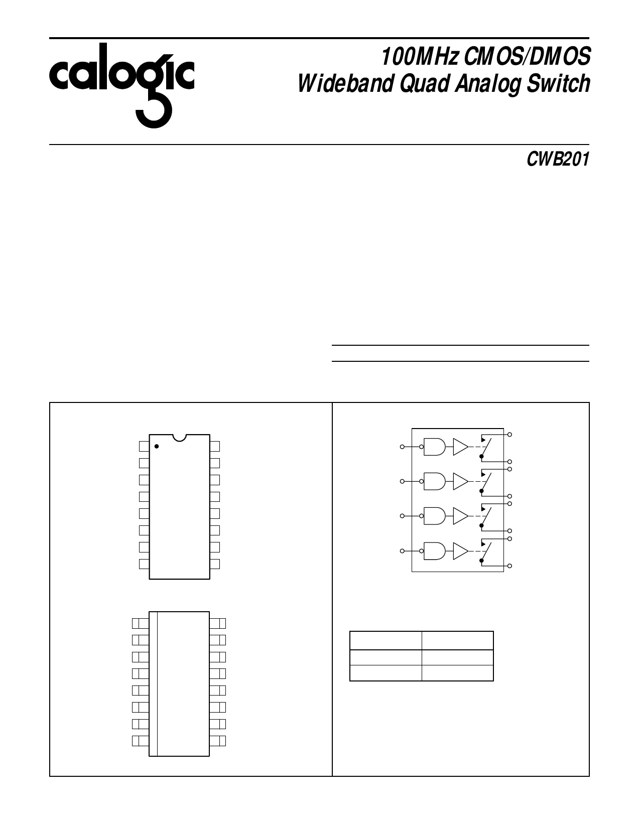
PIN CONFIGURATION
CWB201CP
IN1 1
16 IN2
D1 2
15 D2
S1 3
14 S2
V- 4
13 V+
GND 5
12 N/C
S4 6
11 S3
D4 7
10 D3
IN4 8
9 IN3
TOP VIEW
CWB201CY
IN1 1
16 IN2
D1 2
S1 3
15 D2
14 S2
V- 4
GND 5
13 V+
12 N/C
S4 6
D4 7
11 S3
10 D3
IN4 8
9 IN3
CWB
TOP VIEW
DESCRIPTION
Designed for RF and Video Switching the CWB201 is
manufactured using Calogic’s high speed CMOS combined
with DMOS transistors in a monolithic design resulting in
superior performance characteristics. This quad SPST switch
array has extensive applications where high frequency video,
audio or digital signals are switched or routed. The CWB201
is TTL compatible which is of great benefit to to designs that
require constant logic switching over a wide range of supply
voltages and temperature without a separate power supply.
ORDERING INFORMATION
Part
CWB201CP
CWB201CY
XCWB201
Package
Temperature Range
Plastic 16-Pin Dip
0 to +85oC
Plastic SO-16 Surface Mount 0 to +85oC
Sorted Chips in Carriers
0 to +85oC
FUNCTIONAL BLOCK DIAGRAM
S1
IN 1
D1
S2
IN2
D2
S3
IN3
D3
S4
IN4
D4
Four SPST Switches per Package.
Switches shown in Logic '1' Input Position.
LOGIC TABLE
Logic
0
1
Switch
ON
OFF
Logic ’0’ ≤ 0.8V
Logic ’1’ ≥ 2.42V
NOTE: All devices contain diodes to protect inputs against
damage due to high static voltages or electric fields;
however, it is advised that precautions be taken not to
exceed the maximum recommended input voltages. All
unused inputs must be connected to an appropriate logic
level (VDD or GND).