MC13282AP 데이터 시트보기 (PDF) - Motorola => Freescale
부품명
상세내역
제조사
MC13282AP Datasheet PDF : 12 Pages
| |||
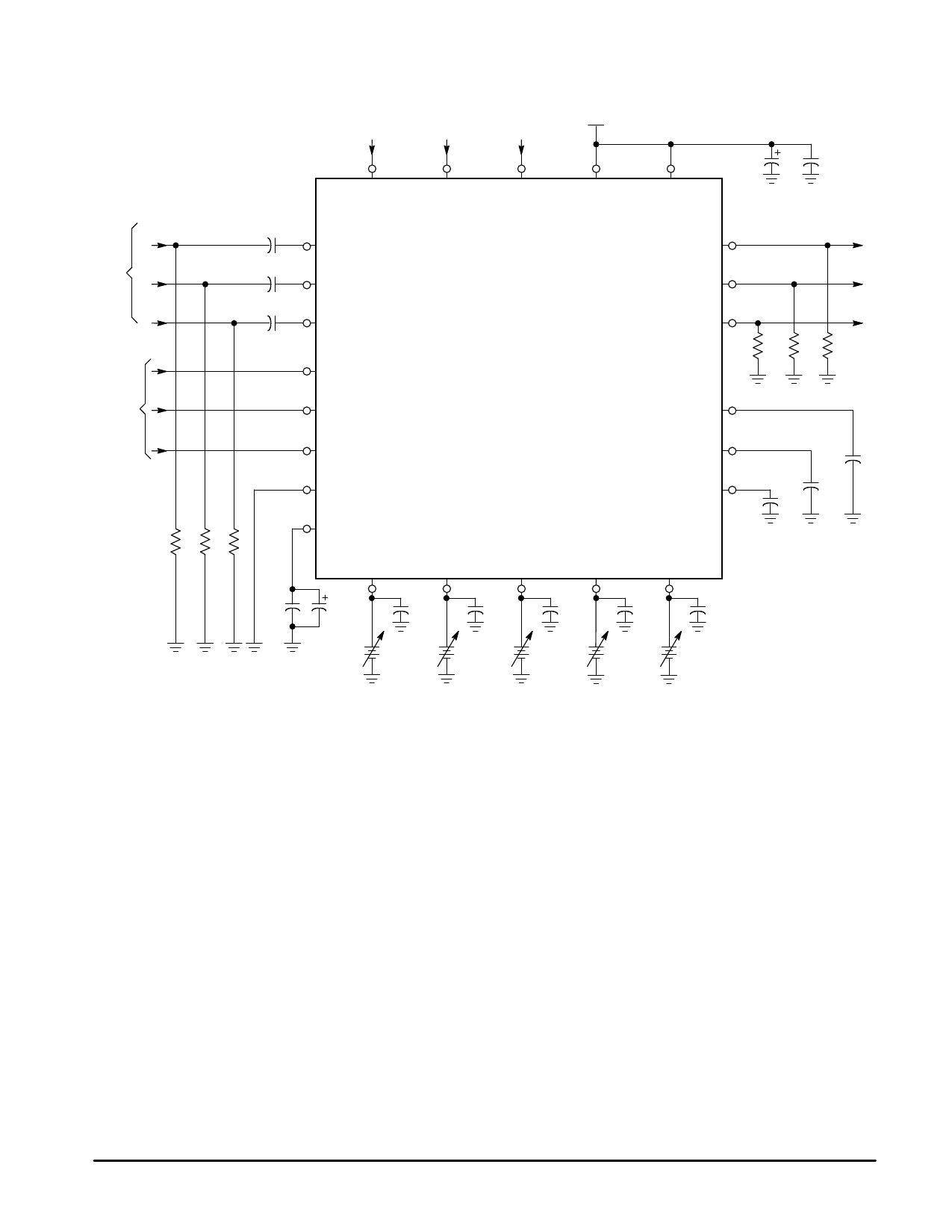
MC13282A
R Input
Video
Inputs
G Input
B Input
OSD
Inputs
R1 R2 R3
75 75 75
Figure 2. Test Circuit
Blank
Input
Clamp
OSD
8.0 V
Input
Select
24
23
14
17
Blank
Clamp
Fast
Commutate
Video
VCC
C1
0.1
2
R Input
C2
0.1
4
G Input
C3
0.1
6
B Input
8 ROSD
10 GOSD
MC13282A
C14
C15
9
47 µF
0.1
VCC
R Emitter 22
R Output
19
G Emitter
15
B Emitter
R4
330
G Output
B Output
R5 R6
330 330
21
R Clamp
12 BOSD
G Clamp 18
7
Gnd
20
V5
16
B Clamp
C11
0.1
Subcontrast Control
R
G
B
OSD
Contrast
Contrast
1
3
5
11
13
C5
C6
C7
C8
C9
C10
C4
10 µF
0.1
0.1
0.1
0.1
0.1
0.1
5.0 V
5.0 V
5.0 V
5.0 V
5.0 V
C13
C12 0.1
0.1
Clamp Capacitor
APPLICATION INFORMATION
PCB Layout
Care should be taken in the PCB layout to minimize the
noise effects. The most sensitive pins are VCC (9), Video VCC
(17), V5 (20), Clamp (16, 18, 21). It is strongly recommended
to make a ground plane and connect VCC/Video VCC and
ground traces to the power supply directly. Separate power
supply traces, should be used for VCC and Video VCC and
decoupling capacitors should be connected as close as
possible to the device. Multi–layer ceramic and tantalum
capacitors are recommended. Pin 20 (V5) is designed as a
5.0 V voltage reference for contrast, RGB subcontrast and
OSD contrast controls, so the same precaution for VCC
should be also applied at this pin. The Clamp capacitors at
Pins 16,18 and 21 should be connected to ground close to
IC’s ground Pin 7 or power supply ground. The copper trace
of the video signal inputs and outputs should be as short as
possible and separated by ground traces to avoid any RGB
cross–interference. A double sided PCB should be used to
optimize the device’s performance.
RGB Input and Output
The RGB output stages are designed as emitter–followers
to drive the CRT driver circuitry directly. The emitter resistors
used is 330 Ω (typically) and the driving current is 15 mA
maximum for each channel. The loading impedance
connected to the output stages should be greater than 330 Ω
and less than 5.0 pF for optimum performance (e.g., rise/fall
time, bandwidth, etc.). Decreasing the resistive load will
reduce the rise/fall time by increasing the driving current, but
the output stage may be damaged due to increasing power
dissipation at the same time. The frequency response is
affected by the loading capacitance. The typical value is 3.0
to 5.0 pF. Figure 4 shows a typical interface with a video output
driver. For a high resolution color monitor application, it is
recommended to use coaxial cable or shielded cable for input
signal connections.
Clamp and Blank Input
The clamp input is normally (except for Sync–on–Green)
connected to a positive horizontal sync pulse, and has a
threshold level of 3.75 V. It is used as a timing reference for
the dc restoration process, so it cannot be left open. If
Sync–on–Green timing mode is used, the clamping pulse
should be located at horizontal back porch period instead of
horizontal sync tip. Otherwise, the black level will be clamped
at an incorrect voltage.
The blank input is used as a video mute, or horizontal
blanking control, and is normally connected to a blanking
MOTOROLA ANALOG IC DEVICE DATA
7
Share Link: 