HI2302 데이터 시트보기 (PDF) - Intersil
부품명
상세내역
제조사
HI2302 Datasheet PDF : 16 Pages
| |||
Pin Descriptions (Continued)
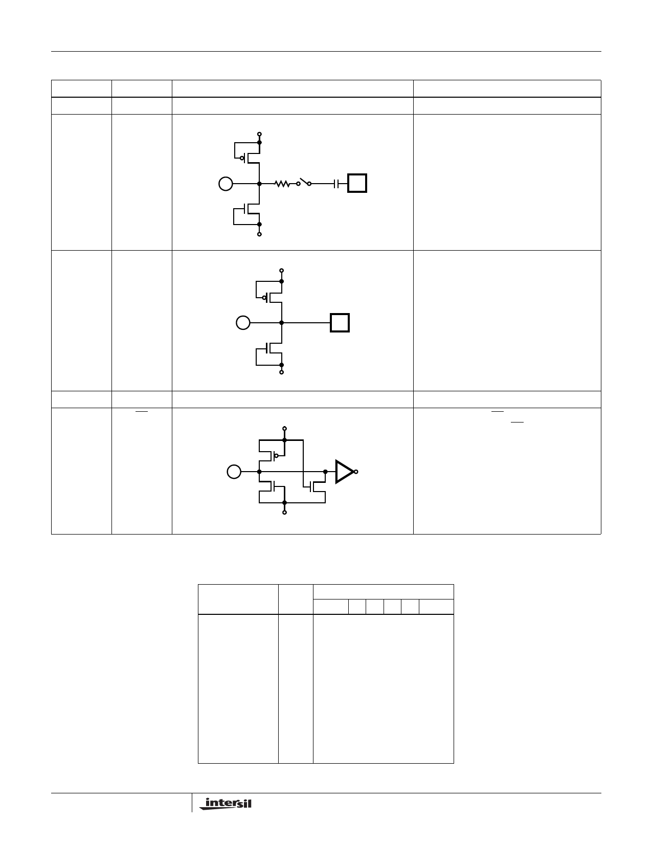
PIN NO.
SYMBOL
22, 23
26
AVSS
VREF
HI2302
EQUIVALENT CIRCUIT
AVDD
27
CCP
26
AVSS
AVDD
27
DESCRIPTION
Analog Ground.
Clamp Reference Voltage Input. Clamps so that
the reference voltage and the input signal during
clamp interval are equal.
Integrates the clamp control voltage. The
relationship between the changes in CCP
voltage and in VIN voltage is positive phase.
28, 31
30
DVSS
OE
AVSS
AVDD
30
Digital Ground.
Data is output when OE = Low. Pins D0 to D7 are
at high impedance when OE = High. Pull-down
resistor is built in.
AVSS
Digital Output
The following table shows the relationship between analog input voltage and digital output code.
INPUT SIGNAL
VOLTAGE
VRT
•
•
•
•
•
•
•
•
VRB
STEP
0
•
•
•
127
128
•
•
•
255
DIGITAL OUTPUT CODE
MSB
LSB
11111111
•
•
•
10000000
01111111
•
•
•
00000000
8
Share Link: 