PM25LV010 데이터 시트보기 (PDF) - PMC-Sierra
부품명
상세내역
제조사
PM25LV010 Datasheet PDF : 24 Pages
| |||
PMC
Pm25LV512/010
WRITE ENABLE (WREN): The device will power up in the write disable state when Vcc is applied. All write
instructions must therefore be preceded by the WREN instruction.
WRITE DISABLE (WRDI): To protect the device against inadvertent writes, the WRDI instruction disables all write
commands. The WRDI instruction is independent of the status of the WP# pin.
READ STATUS REGISTER (RDSR): The RDSR instruction provides access to the status register. The READY/
BUSY and write enable status of the device can be determined by the RDSR instruction. Similarly, the Block Write
Protection bits indicate the extent of protection employed. These bits are set by using the WRSR instruction.
During internal write cycles, all other commands will be ignored except the RDSR instruction.
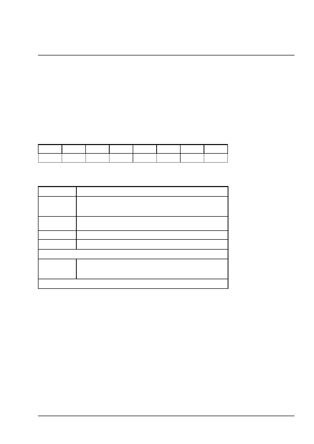
Table 3. Status Register Format
Bit 7
WPEN
Bit 6
X
Bit 5
X
Bit 4
X
Bit 3
BP1
Bit 2
BP0
Bit 1
WEN
Bit 0
RDY
Table 4. Read Status Register Bit Definition
Bit
Definition
Bit 0 (RDY)
Bit 1 (WEN)
Bit 2 (BP0)
Bit 0 = 0 indicates the device is READY.
Bit 0 = 1 indicates the write cycle is in progress and the device is
BUSY.
Bit 1 = 0 indicates the device is not WRITE ENABLED.
Bit 1 = 1 indicates the device is WRITE ENABLED.
See Table 5.
Bit 3 (BP1)
See Table 5.
Bits 4-6 are 0s when device is not in an internal write cycle.
Bit 7 (WPEN)
WPEN = 0 blocks the function of Write Protect pin (WP#).
WPEN = 1 activates the Write Protect pin (WP#).
See Table 6 for details.
Bits 0-7 are 1s during an internal write cycle.
WRITE STATUS REGISTER (WRSR): The WRSR instruction allows the user to select one of four levels of protec-
tion for the Pm25LV010. The Pm25LV010 is divided into four blocks where the top quarter (1/4), top half (1/2), or all
of the memory blocks can be protected (locked out) from write. The Pm25LV512 is divided into 2 blocks where all
of the memory blocks can be protected (locked out) from write. Any of the locked-out blocks will therefore be READ
only. The locked-out block and the corresponding status register control bits are shown in Table 5.
The three bits, BP0, BP1, and WPEN, are nonvolatile cells that have the same properties and functions as the
regular memory cells (e.g., WREN, RDSR).
Programmable Microelectronics Corp.
8
Issue Date: December, 2003, Rev: 1.3
Share Link: 