ADM1020AR-REEL 데이터 시트보기 (PDF) - Analog Devices
부품명
상세내역
제조사
ADM1020AR-REEL Datasheet PDF : 12 Pages
| |||
ADM1020
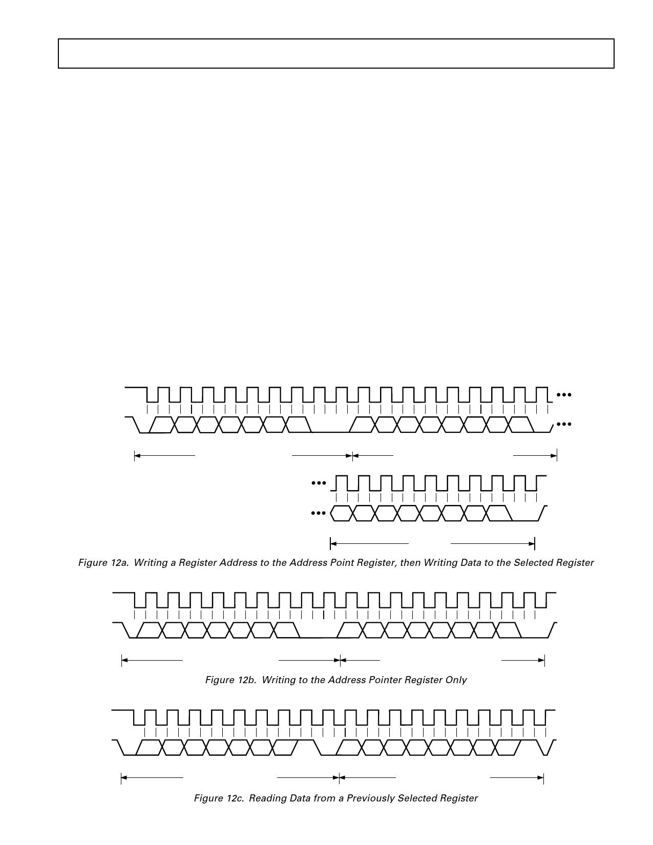
In the case of the ADM1020, write operations contain ei-
ther one or two bytes, while read operations contain one
byte, and perform the following functions:
To write data to one of the device data registers or read data
from it, the Address Pointer Register must be set so that the
correct data register is addressed, then data can be written
into that register or read from it. The first byte of a write
operation always contains a valid address that is stored in
the Address Pointer Register. If data is to be written to the
device, then the write operation contains a second data byte
that is written to the register selected by the address pointer
register.
This is illustrated in Figure 12a. The device address is sent over
the bus followed by R/W set to 0. This is followed by two data
bytes. The first data byte is the address of the internal data
register to be written to, which is stored in the Address Pointer
Register. The second data byte is the data to be written to the
internal data register.
When reading data from a register there are two possibilities:
1. If the ADM1020's Address Pointer Register value is un-
known or not the desired value, it is first necessary to set it
to the correct value before data can be read from the desired
data register. This is done by performing a write to the
ADM1020 as before, but only the data byte containing the
1
SCLK
register read address is sent, as data is not to be written to
the register. This is shown in Figure 12b.
A read operation is then performed consisting of the serial bus
address, R/W bit set to 1, followed by the data byte read from
the data register. This is shown in Figure 12c.
2. If the Address Pointer Register is known to be already at the
desired address, data can be read from the corresponding
data register without first writing to the Address Pointer
Register, so Figure 12b can be omitted.
NOTES
1. Although it is possible to read a data byte from a data register
without first writing to the Address Pointer Register, if the
Address Pointer Register is already at the correct value, it is
not possible to write data to a register without writing to the
Address Pointer Register, because the first data byte of a
write is always written to the Address Pointer Register.
2. Don't forget that the ADM1020 registers have different ad-
dresses for read and write operations. The write address of a
register must be written to the address pointer if data is to be
written to that register, but it is not possible to read data
from that address. The read address of a register must be
written to the address pointer before data can be read from
that register.
9
1
9
SDATA
A6
START BY
MASTER
A5 A4 A3 A2 A1 A0 R/W
D7
FRAME 1
SERIAL BUS ADDRESS BYTE
ACK. BY
ADM1020
1
SCL (CONTINUED)
D6 D5 D4 D3 D2 D1 D0
FRAME 2
ADDRESS POINTER REGISTER BYTE
ACK. BY
ADM1020
9
SDA (CONTINUED)
D7 D6 D5 D4 D3 D2 D1 D0
FRAME 3
DATA BYTE
ACK. BY STOP BY
ADM1020 MASTER
Figure 12a. Writing a Register Address to the Address Point Register, then Writing Data to the Selected Register
1
9
1
9
SCLK
SDATA
A6
START BY
MASTER
A5 A4 A3 A2 A1 A0 R/W
D7 D6 D5 D4 D3 D2 D1 D0
FRAME 1
SERIAL BUS ADDRESS BYTE
ACK. BY
ADM1020
FRAME 2
ADDRESS POINTER REGISTER BYTE
ACK. BY STOP BY
ADM1020 MASTER
Figure 12b. Writing to the Address Pointer Register Only
1
9
1
9
SCLK
SDATA
A6
START BY
MASTER
REV. 0
A5 A4 A3 A2 A1 A0 R/W
D7 D6 D5 D4 D3 D2 D1
FRAME 1
SERIAL BUS ADDRESS BYTE
ACK. BY
ADM1020
FRAME 2
DATA BYTE FROM ADM1020
Figure 12c. Reading Data from a Previously Selected Register
–9–
D0
NO ACK. STOP BY
BY MASTER MASTER
Share Link: 