RE46C146 데이터 시트보기 (PDF) - R and E International, Inc.
부품명
상세내역
제조사
RE46C146
R and E International, Inc.

RE46C146 Datasheet PDF : 12 Pages
| |||
RE46C146
CMOS Photoelectric Smoke Detector ASIC with Intelligent IO and Timer Mode
Preliminary Product Specification
R&E International
Low Battery and Chamber Test – In standby an internal reference is compared to the voltage divided VDD supply.
Low battery status is latched at the conclusion of the LED pulse. The horn will chirp for 10ms every 43 seconds
until the low battery condition no longer exists. In standby a chamber test is also performed every 40 seconds by
switching to the high gain capacitor C1 and sensing the photo chamber background reflections. Two consecutive
chamber tests failures will also cause the horn to chirp for 10mS every 43 seconds. The low battery chirp occurs
next to the LED pulse and the failed chamber test chirp ~20 seconds later. The low battery and chamber tests are
not performed in a local or remote alarm condition.
Timer Mode – If resistors Radj1 and Radj2 are in place and a high to low transition occurs on the TEST input the
device enters a 10 minute timer mode. In this mode the smoke comparator reference is switched from the internal
VDD-3.5V reference to the voltage that appears on VSEN (pin 15). This allows the sensitivity to be modified for
the duration of the 10 minute timer period. The chamber test is not performed in the timer mode. If VSEN is left
unconnected or tied to VSS the timer mode of operation is inhibited.
Diagnostic Mode – In addition to the normal function of the TEST input a special diagnostic mode is available for
calibration and test of the smoke detector. Taking the TEST pin below VSS and sourcing ~300uA out of the pin
for 1 clock cycle will enable the diagnostic mode. In the diagnostic mode some of the pin functions are redefined.
Refer to the table below for redefined pin functions in the diagnostic mode. In addition in this mode STROBE is
always enabled and the IRED is pulsed at the clock rate of 10.5mS nominal.
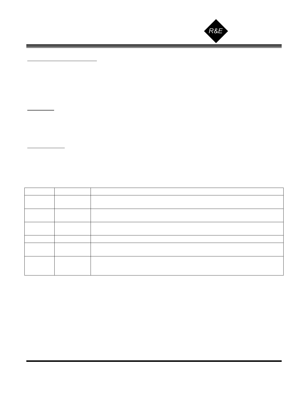
Pin Name
IO
VSEN
FEED
COSC
HORNB
LED
Pin Number
7
15
10
12
8
11
Description
The IO pin (7) controls the gain capacitor used for the photo amplifier. If IO is low
then normal gain is selected. If IO is high then high gain is selected.
In diagnostic mode the output of the photo amplifier is gated to this pin and the pull
down device is disabled.
If VSEN (15) is low then taking this input high will enable hysteresis which is a
nominal 10% gain increase in normal gain mode.
If desired this pin can be driven by an external clock.
This pin becomes the smoke integrator output. A high level indicates that an alarm
condition has been detected.
The LED pin is used as a low battery indicator. For VDD above the low battery
threshold the open drain NMOS is off. If VDD falls below the threshold the NMOS
turns on.
Telephone 610.992.0727
Facsimile 610.992.0734
E-mail: rande@randeint.com
Page 9 of 12
DS-RE46C146-060605
This datasheet contains PROPRIETARY and CONFIDENTIAL information.
Share Link: