RF2374PCBA-411(V2) 데이터 시트보기 (PDF) - RF Micro Devices
부품명
상세내역
제조사
RF2374PCBA-411 Datasheet PDF : 8 Pages
| |||
RF2374
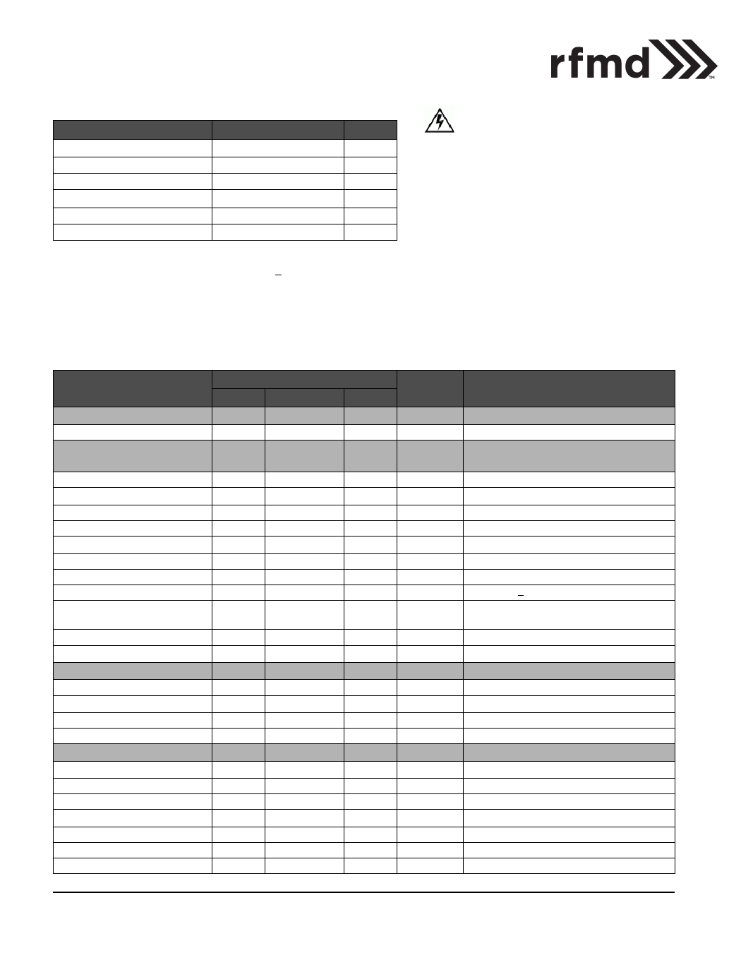
Absolute Maximum Ratings
Parameter
Rating
Unit
Supply Voltage
-0.5 to +6.0
VDC
Input RF Level
+5 (see note)
dBm
Current Drain, ICC
32
mA
Operating Ambient Temperature
-40 to +85
°C
Storage Temperature
-40 to +150
°C
NOTE: Exceeding any one or a combination of the above maximum rating lim-
its may cause permanent damage. Input RF transients to +15dBm will not
harm the device. For sustained operation at inputs >+5dBm, a small dropping
resistor is recommended in series with the VCC in order to limit the current due
to self-biasing to <32mA.
Caution! ESD sensitive device.
The information in this publication is believed to be accurate and reliable. How-
ever, no responsibility is assumed by RF Micro Devices, Inc. ("RFMD") for its use,
nor for any infringement of patents, or other rights of third parties, resulting
from its use. No license is granted by implication or otherwise under any patent
or patent rights of RFMD. RFMD reserves the right to change component cir-
cuitry, recommended application circuitry and specifications at any time without
prior notice.
RoHS status based on EUDirective2002/95/EC (at time of this document revi-
sion).
Parameter
Operating Range
Frequency Range
WLAN Low Noise Amplifier
Frequency
HIGH GAIN MODE
Gain
Noise Figure
Input IP3
IP1dB
Current Drain
BYPASS MODE (Low Gain)
Gain
Input IP3
Current Drain
GPS Low Noise Amplifier
Frequency
Gain
Noise Figure
Input IP3
WiMAX Low Noise Amplifier
Frequency
Gain
Noise Figure
Input IP3
CDMA Low Noise Amplifier
HIGH GAIN MODE
Frequency
Gain
Noise Figure
Input IP3
Current Drain
Specification
Min.
Typ.
Max.
800
4000
2450
13.5
14.5
1.3
1.5
+7
+9
0
7
-4.0
-3.0
-2.0
+19
+21
2.0
3.0
1575
17.5
1.0
+7.0
3500
11.0
1.6
+10.0
869
894
19
1.0
+2.0
7
Unit
MHz
Condition
TAMB=+25°C, VCC=3.0V
MHz
dB
dB
dBm
dBm
mA
dB
dBm
mA
Gain Select<0.8V, VREF=3V, T=+25°C
IIP3 will improve if ICC is raised above 7mA.
Gain Select>1.8V
Note: Bypass mode insertion loss will degrade
gradually as VCC goes below 2.7V.
MHz
dB
dB
dBm
ICC = 7 mA
MHz
dB
dB
dBm
ICC = 7 mA
At 3500MHz
At 3500MHz
IIP3 will improve if ICC is raised above 7mA.
MHz
dB
dB
dBm
IIP3 will improve if ICC is raised above 7mA.
mA
2 of 8
7628 Thorndike Road, Greensboro, NC 27409-9421 · For sales or technical
support, contact RFMD at (+1) 336-678-5570 or sales-support@rfmd.com.
Rev A0 DS070705
Share Link: 