RF2374PCBA-411(V2) 데이터 시트보기 (PDF) - RF Micro Devices
부품명
상세내역
제조사
RF2374PCBA-411 Datasheet PDF : 8 Pages
| |||
RF2374
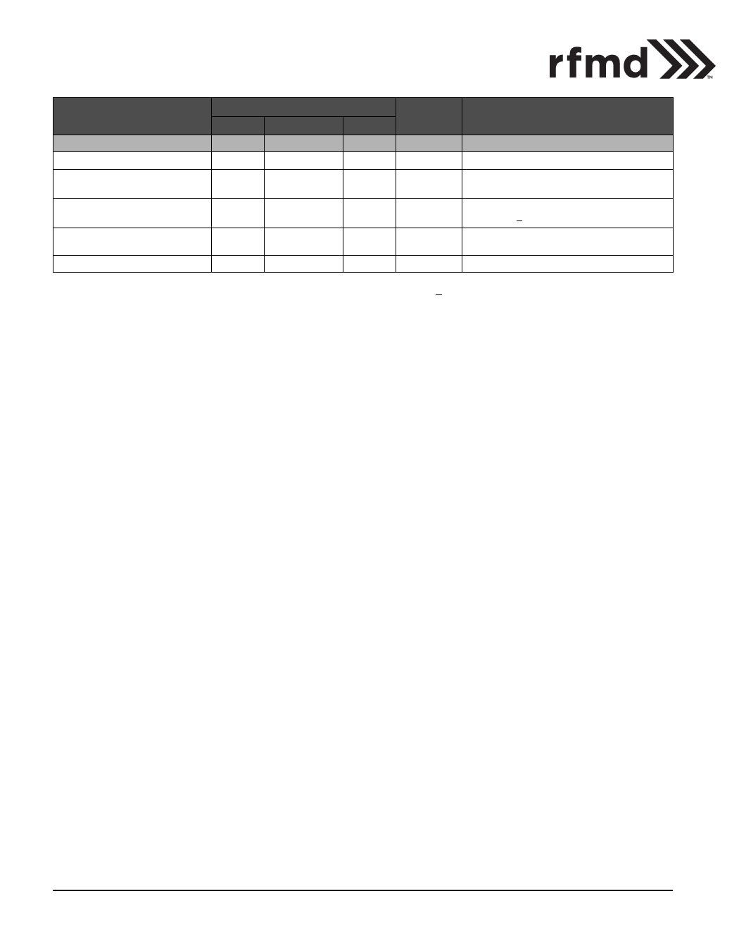
Pin Function Description
Interface Schematic
1
RF IN
RF input pin. This part is designed such that 50Ω is the optimal source
impedance for best noise figure. Best noise figure is achieved with only a
series capacitor on the input.
To Bias
Circuit
RF OUT
RF IN
2
GND1
Ground connection. For best performance, keep traces physically short
and connect immediately to ground plane.
3
VREF
For low noise amplifier applications, this pin is used to control the bias cur-
rent. An external resistor can be used to set the bias current for any VBIAS
voltage. This device will have good gain and noise figure with ICC as low as
3 mA.
VREF
4 GAIN SELECT This pin selects high gain and bypass modes.
Gain Select<0.8V, high gain.
Gain Select>1.8V, low gain.
5
GND2
See GND1.
6
7
8
Pkg
Gnd
RF OUT
NC
NC
GND
Amplifier output pin. This pin is an open-collector output. It must be biased
to VCC through a choke or matching inductor.
Not connected.
Not connected.
This pad should be connected to the ground plane by vias directly under
the device.
INDEX
AREA
2.20
Package Drawing
2 PLCS
0.10 C
0.10 C
2 PLCS
0.63
0.53
0.152
REF
B
A
2.20
0.65
0.05
0.00
SEATING
PLANE
C
0.10
MAX
11..2000TYP
Dimensions in mm.
Shaded lead is pin 1.
0.31
0.21
0.28
0.18
0.10 M C A B
4 of 8
7628 Thorndike Road, Greensboro, NC 27409-9421 · For sales or technical
support, contact RFMD at (+1) 336-678-5570 or sales-support@rfmd.com.
Rev A0 DS070705
Share Link: 