RF3145 데이터 시트보기 (PDF) - RF Micro Devices
부품명
상세내역
제조사
RF3145 Datasheet PDF : 18 Pages
| |||
RF3145
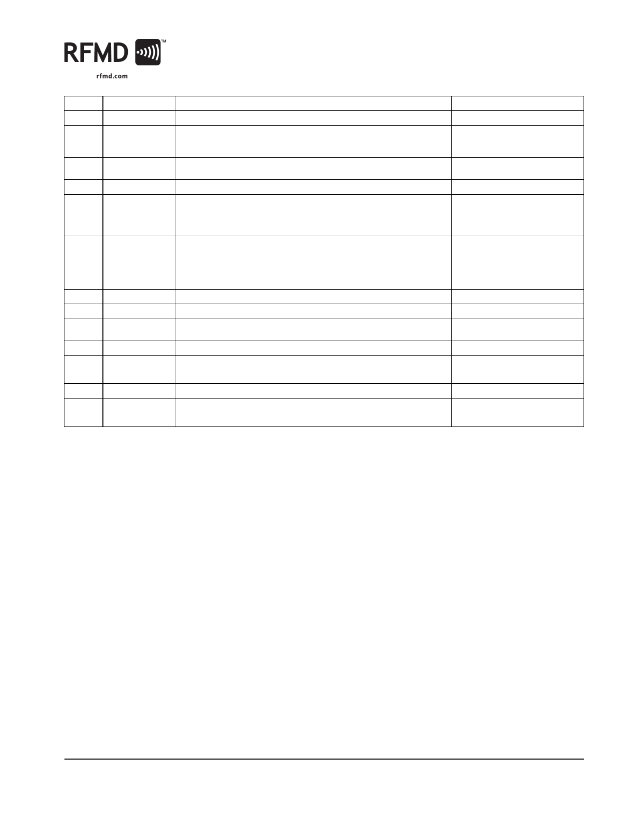
Pin
1
2
3
4
5
6
7
8
9
10
11
12
Pkg
Base
Function
DCS/PCS IN
BAND SELECT
TX ENABLE
VBATT
VMODE
VRAMP
GSM IN
NC
GSM OUT
NC
DCS/PCS
OUT
NC
GND
Description
RF input to the DCS/PCS band. This is a 50Ω input.
Allows external control to select the GSM or DCS/PCS band with a logic
high or low. A logic low enables the GSM band whereas a logic high
enables the DCS/PCS band.
This signal enables the PA module for operation with a logic high. Once TX
Enable is asserted the RF output level will increase to 0dBm.
Power supply for the module. This should be connected to the battery.
This signal selects 8PSK mode with a logic “high” (1.5V to 3.0V), and
selects GMSK mode with a logic “low” (0V to 0.7V). When the VMODE
switch is enabled “high”, the gain in the GSM band is reduced by bypassing
the first stage amplifier. When the VMODE is “low”, all stages are active.
Ramping signal from DAC. A simple RC filter may need to be connected
between the DAC output and the VRAMP input depending on the baseband
selected. The ramping profiles shown later in the data sheet are recom-
mended profiles for meeting the GSM specification for burst timing and
transient spectrum.
RF input to the GSM band. This is a 50Ω input.
Not connected.
RF output for the GSM band. This is a 50Ω output. The output load line
matching is contained internal to the package.
Not connected.
RF output for the DCS/PCS band. This is a 50Ω output. The output load
line matching is contained internal to the package.
Not connected.
Interface Schematic
Rev A4 DS050919
7628 Thorndike Road, Greensboro, NC 27409-9421 · For sales or technical
support, contact RFMD at (+1) 336-678-5570 or sales-support@rfmd.com.
9 of 18
Share Link: 