RMPA1852 데이터 시트보기 (PDF) - Fairchild Semiconductor
부품명
상세내역
제조사
RMPA1852 Datasheet PDF : 11 Pages
| |||
ADVANCED DATA SHEET
Electrical Specifications (Continued)
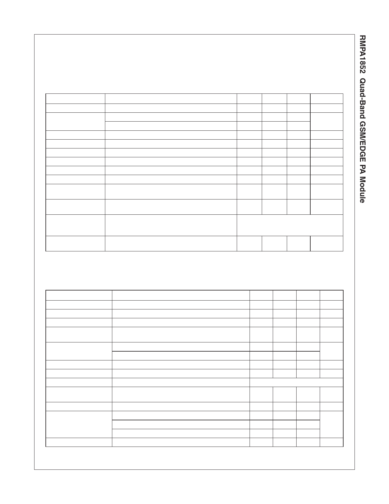
Mode: GMSK Band: DCS Tx band (1710–1785 MHz)
Modulation: None (CW), Typical Peak/Average = 0dB
Pulse Rate: TX = 577µs, 25% duty cycle, Tframe = 4.615mS
Test conditions unless otherwise stated: Vcc = 3.5V, Vramp = Vramp Max., Zin = Zout = 50Ω, Pin = 3 dBm, Temperature = 25°C,
Duty Cycle = 25%
Parameter
Test Conditions
Frequency
DCS
Output Power
Temp = 25°C, Vcc = 3.5 V
Temp = 85°C, Vcc = 2.9 V
Input Power Range
Power Added Efficiency
At Pout max
Input VSWR
Pout = 0 to 35 dBm
Forward Isolation
Pin = 6 dBm
Power Control Range
Vramp = 0.2 to 1.8 V
Harmonics
Stability
Load 6:1, all phase angles, Pin = 3 dBm, Set Vramp
where Pout less than or equal to 32 dBm into a 50Ω load.
Noise Power
Ftx = 1710–1785, Frx = 1805–1880 MHz
(RBW = 100 KHz)
Ruggedness
Output VSWR = 10:1, All phase angles, Vcc = 4.8 V,
Pin = 3 dBm, Set Vramp where Pout less than or equal to
32 dBm into a 50Ω load.
Output Power Switching
Speed
RF Pout 5–35 dBm to within 1 dB of final value.
Min
1710
32
29.5
+0
45
–
–
–
–
–
–
–
Typ
–
33
–
+3
50
–
-35
40
–
–
Max
1785
–
–
+6
–
2.5:1
–
-5
-36
–
-77
No Damage
–
2
Unit
MHz
dBm
dBm
%
Ratio
dBm
dB
dBm
dBm
dBm
µS
Mode: EDGE Band: DCS Tx band (1710–1785 MHz)
Modulation: EDGE modulation (3π/8 O-8PSK at 270.833 ksps), Max Peak/Avg = 3.3dB (Probability < 0.1%).
Pulse Rate: TX = 577µs, 25% duty cycle, Tframe = 4.615mS
Input Power: Adjust to meet Output Power Requirement
Parameter
Test Conditions
Min Typ Max
Duty Cycle
1/8
1/4
1/4
Output Power
Max Pi = -0.5 (Temp = 25°C, Vcc = 3.5 V)
–
28
–
Power Added Efficiency
(Temp = 25°C, Vcc = 3.5 V)
–
26
–
Low power current
Pout<16 dBm
200
consumption mode (L)
Gain
at Pout (H)
34
at Low power current consumption mode (L)
25
Input VSWR
–
–
2.0:1
Harmonics 2Fo Thru 5Fo
At Max Po (Temp = 25°C, Vcc = 3.5 V)
–
–
-10
Ruggedness
VSWR = 10:1, All phase angles, Vcc = 4.8 V, Max Pin = 8
No Damage
Stability
All Spurious (Load VSWR = 6:1 at all angles
Po < 28, Pin < 8 dBm)
–
–
-65
TX Noise in RX Band
Ftx = 1710–1785, Frx = 1805–1880 MHz (RBW = 100 KHz) –
–
-77
Adjacent Channel Leakage
Offset: ±200 KHz
–
–
-33
Offset: ±400 KHz
–
-57
Offset: ±600 KHz
–
–
-60
Error Vector Magnitude
Load 50Ω
–
–
4
Unit
dBm
%
mA
dB
Ratio
dBm
dBc
dBm
dBc
%
RMPA1852 Rev. C
5
www.fairchildsemi.com
Share Link: 