RT8805 데이터 시트보기 (PDF) - Richtek Technology
부품명
상세내역
제조사
RT8805 Datasheet PDF : 15 Pages
| |||
RT8805
Preliminary
LGATE. OCP function monitors both channels, either
one can activate OCP. If the OC protection occurs three
times, OCSD (Over Current Shut Down) will be activated
and shut down the chip.
e. When fault conditions occur or SS < 0.4V, the current
sense function will be disabled.
Power Good
PGOOD goes high when soft-start voltage > 3.7V, and no
fault conditions.
Feedback Loop Compensation
The RT8805 is a voltage mode controller ; the control
loop is a single voltage feedback path including an error
amplifier and PWM comparator. In order to achieve fast
transient response and accurate output regulation, an
adequate compensator design is necessary. The goal of
the compensation network is to provide adequate phase
margin (greater than 45 degrees) and the highest 0dB
crossing frequency. To manipulate loop frequency response
under its gain crosses over 0dB at a slope of -20dB/
decade.
1) Modulator Frequency Equations
RT8805 is a voltage mode buck converter using the high
gain error amplifier with transconductance (OTA,
Operational Transconductance Amplifier), as Figure 6
shown.
The Transconductance:
GM =
ΔIOUT
ΔVM
Δ VM = (EA+) - (EA-) ; Δ IOUT = E/A output current.
EA+ +
EA- -
GM
VOUT
ROUT
Figure 6. OTA Topology
This transfer function of OTA is dominated by a higher DC
gain and the output filter (LOUT and COUT) with a double
pole frequency at FLC and a zero at FESR. The DC gain of
the modulator is the input voltage (VIN) divided by the
peak to peak oscillator voltage VRAMP.
www.richtek.com
10
The first step is to calculate the complex conjugate poles
contributed by the LC output filter.
The output LC filter introduces a double pole, 40dB/decade
gain slope above its corner resonant frequency, and a total
phase lag of 180 degrees. The resonant frequency of the
LC filter expressed as follows:
FP(LC) =
1
2π × LOUT × COUT
The next step of compensation design is to calculate the
ESR zero. The ESR zero is contributed by the ESR
associated with the output capacitance. Note that this
requires that the output capacitor should have enough ESR
to satisfy stability requirements. The ESR zero of the
output capacitor expressed as follows:
FZ(ESR)
=
2π
1
× COUT
× ESR
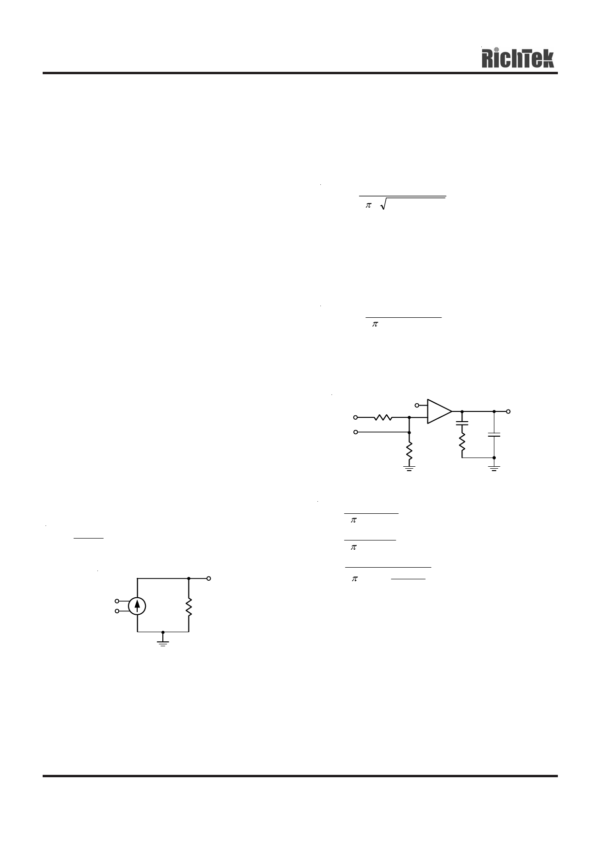
2) Compensation Frequency Equations
The compensation network consists of the error amplifier
and the impedance networks ZC and ZF as Figure 7 shown.
VOUT
FB
R1 VREF
+
GM
-
C2
VCOMP
C1
R2
RF
Figure 7. Compensation Loop
FZ1
=
2π
1
×R2× C2
FP1
=
2π
1
×R1× C1
FP2
=
2π
1
×
R2
×
⎜⎝⎛
C1×
C1+
C2
C2
⎟⎠⎞
Figure 8 shows the DC-DC converter's gain vs. frequency.
The compensation gain uses external impedance networks
ZC and ZF to provide a stable, high bandwidth loop. High
crossover frequency is desirable for fast transient
response, but often jeopardize the system stability. In
order to cancel one of the LC filter poles, place FZ1 before
the LC filter resonant frequency. In the experience, place
FZ1 at 10% LC filter resonant frequency. Crossover
frequency should be higher than the ESR zero but less
than 1/5 of the switching frequency. The FP2 should be
place at half the switching frequency.
DS8805-01 November 2005
Share Link: 