RT8855 데이터 시트보기 (PDF) - Richtek Technology
부품명
상세내역
제조사
RT8855 Datasheet PDF : 18 Pages
| |||
RT8855
Application Information
The RT8855 is a dual output PWM controller supports
hybrid power control of AMD processors which operate
from either a 6-bit parallel VID interface (PVI) or a serial
VID interface (SVI). One of the outputs is a 4/3/2/1-phase
PWM controller with two integrated MOSFET drivers to
support CPU core voltage (VDD) and another is a single-
phase buck controller with an integrated MOSFET driver
to power North-Bridge (NB) chipset (VDDNB) in SVI mode.
In PVI mode, only multiphase PWM controller is active
for single-plane VDD only processor.
Richtek's proprietary Burst Transient Response(BTRTM),
provides fastest initial response to high di/dt load transients
and less bulk and ceramic output capacitance is required
to meet transient regulation specifications. The RT8855
incorporates differential voltage sensing, continuous
inductor DCR phase current sensing, programmable load-
line voltage positioning and offset voltage to provide high
accuracy regulated power for both VDD and VDDNB. While
VDDNB is enabled in SVI mode, it will be automatically
phase-shifted with respect to the CPU Core phases in
order to reduce the total input RMS current amount.
CPU_TYPE Detection and System Start-Up
At system Start-up, on the rising-edge of EN signal,
RT8855 monitors the status of VID1 and latches the PVI
mode (VID1 = 1) or SVI mode (VID1 = 0).
PVI Mode
PVI is a 6-bit-wide parallel interface used to address the
CPU Core section reference. According to the selected
code, the device sets the Core section reference and
regulates its output voltage according to Table 2. In this
mode, NB section is kept in high impedance. Furthermore,
PWROK information is ignored as well since the signal
only applies to the SVI protocol.
SVI Mode
SVI is a two wire, Clock and Data, bus that connect a
single master (CPU) to one slave (RT8855). The master
initiates and terminates SVI transactions and drives the
clock, SVC, and the data, SVD, during a transaction. The
slave receives the SVI transactions and acts accordingly.
SVI wire protocol is based on fast-mode I2C as shown in
Figure1. SVI interface also consider two additional signals
needed to manage the system start-up. These signals
are EN and PWROK. The device asserts a PGOOD signal
if the output voltages are in regulation.
Start
Slave Addressing + W
ACK Data Phase ACK Stop
SVC
6 5 4 30
760
SVD
Start
110b
Slave Addressing
(7 Clocks)
ACK
ACK
Write ACK Data Phase ACK Stop
(1Ck) (1Ck) (8 Clocks) (1Ck)
BUS Driven by RT8855
BUS Driven by Master (CPU)
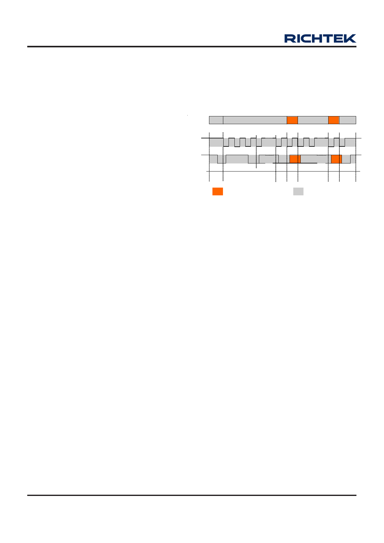
Figure 1. SVI Communication-Send Byte
Set VID Command
The Set VID Command is defined as the command
sequence that the CPU issues on the SVI bus to modify
the voltage level of the Core section and NB section, as
shown is Figure 1. During a Set VID Command, the
processor sends the start (Start) sequence followed by
the address of the Section which the Set VID Command
applies. The processor then sends the write (WRITE) bit.
After the write bit, The Voltage Regulator (VR) sends the
acknowledge (ACK) bit. The processor then sends the
VID bits code during the data phase. The VR sends the
acknowledge (ACK) bit after the data phase. Finally, the
processor sends the stop (Stop) sequence. After the VR
has detected the stop, it performs an On-the-Fly VID
transition for the addressed section(s). Refer to Table 3
for the details of SVI send byte.
RT8855 is able to manage individual power off for both
VCORE and NB sections. The CPU may issue a serial
VID command to power off or power on one section while
the other one remains powered. In this case, the PGOOD
signal remains asserted.
www.richtek.com
10
DS8855-01 April 2011
Share Link: 