RT8855 데이터 시트보기 (PDF) - Richtek Technology
부품명
상세내역
제조사
RT8855 Datasheet PDF : 18 Pages
| |||
RT8855
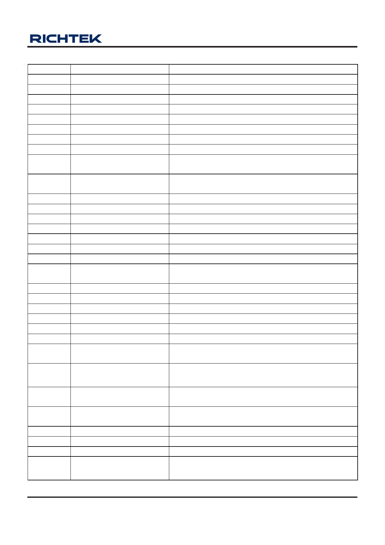
Functional Pin Description
Pin No.
Pin Name
Pin Function
1
PWROK
PWROK Input Signal.
2
RT
Connect this pin to GND by a resistor to adjust frequency.
3
FBRTN
Remote sense ground for CORE.
4
FBRTN_NB
Remote sense ground for NB.
5
FB_NB
Inverting input of error-amp for NB.
6
COMP_NB
Output of error-amp and input of PWM comparator for NB.
7
ISP_NB
Positive current sense pin of NB
8
ISN_NB
Negative current sense pin of NB
9
ADJ
Connect this pin to GND by a resistor to set load line of
VCORE.
10
OFS
11
COMP
12
FB
13
IMAX_NB
Connect this pin to GND/5VCC by a resistor to set no-load
offset voltage of VCORE.
Output of error-amp and input of PWM comparator of VCORE.
Inverting input of error-amp of VCORE.
Connect this pin to GND by a resistor to set OCP of NB.
14
IMAX
Connect this pin to GND by a resistor to set OCP of VCORE.
15, 17, 19, 21 ISN1, ISN2, ISN3, ISN4
Negative current sense pin of channel 1, 2, 3 and 4.
16, 18, 20, 22 ISP1, ISP2, ISP3, ISP4
Positive current sense pin of channel 1, 2, 3 and 4.
23
PS
Power Saving Mode Selection Pin.
24
VCC5
Output of internal 5V regulator for control circuits power supply.
Connect this pin to GND by a ceramic capacitor larger than 1uF.
25,26 PWM4, PWM3
PWM output for channel 4 and channel 3.
27, 35, 36 BOOT2, BOOT1, BOOT_NB
Bootstrap supply for channel 2 and channel 1 and NB.
28, 34, 37 UGATE2, UGATE1, UGATE_NB Upper gate driver for channel 2 and channel 1 and NB.
29, 33, 38 PHASE2, PHASE1, PHASE_NB Switching node of channel 2 and channel 1 and NB.
30, 32, 39 LGATE2, LGATE1, LGATE_NB Lower gate driver for channel 2 and channel 1 and NB.
31, 40 VCC12, VCC12_NB
IC power supply. Connect this pin to 12V.
41
VID0/VFIXEN
42
VID1/PVI
43
VID2/SVD
PVI Mode : Used as voltage identification input for DAC.
SVI Mode : Functions as VFIXEN selection input.
This pin selects PVI/SVI mode based on the state of this pin
prior to EN signal.
PVI Mode : Used as voltage identification input for DAC.
PVI Mode : Used as voltage identification input for DAC.
SVI Mode : Serial data input.
44
VID3/SVC
PVI Mode : Used as voltage identification input for DAC.
SVI Mode : Serial clock input.
45, 46 VID4, VID5
PVI Mode : Used as voltage identification input for DAC.
47
PGOOD
Power Good Indicator (open drain).
48
EN
Exposed pad
(49)
GND
Enable Input Signal.
Reference Ground for the IC. The exposed pad must be
soldered to a large PCB and connected to GND for maximum
power dissipation.
DS8855-01 April 2011
www.richtek.com
5
Share Link: 