RT8856 데이터 시트보기 (PDF) - Richtek Technology
부품명
상세내역
제조사
RT8856 Datasheet PDF : 23 Pages
| |||
RT8856
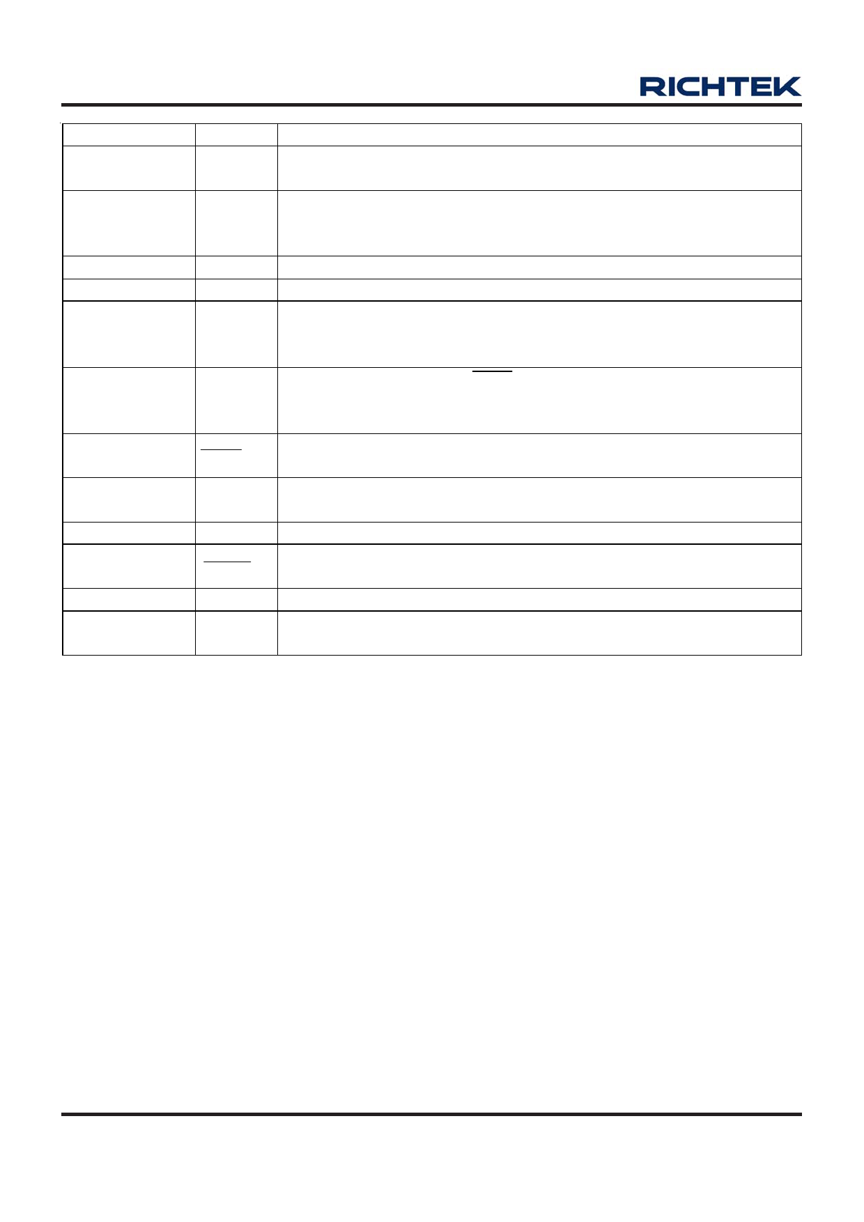
Pin No.
30
31
32
33
34
35
36
37
38
39
40
41 (Exposed Pad)
Pin Name
Pin Function
Upper Gate Drive of Phase2. This pin drives the gate of the high side
UGATE2
MOSFETs.
Bootstrap Power Pin of Phase2. This pin powers the high side MOSFET drivers.
BOOT2 Connect this pin to the junction of the bootstrap capacitor with the cathode of the
bootstrap diode. Connect the anode of the bootstrap diode to the PVCC pin.
ISEN2_N Negative Input of Phase2 Current Sense.
ISEN2 Positive input of Phase2 Current Sense.
Over Current Protection Setting. Connect a resistive voltage divider from VCC to
OCSET ground and connect the joint of the voltage divider to the OCSET pin. The
voltage, VOCSET, determines the over current threshold, ILIM.
Thermal Detection Input for VRTT Circuit. Connect this pin with a resistive
NTC
voltage divider from VCC using NTC on the top to set the thermal management
threshold level.
VRTT
Voltage Regulator Thermal Throttling. This open-drain output pin indicates the
temperature exceeding the preset level when it is pulled low.
TON
Connect this pin to VIN with one resistor. This resistor value sets the ripple size
in ringing free mode.
VCC
Chip Power.
CLKEN
Inverted Clock Enable. This open-drain pin is an output indicating the start of the
PLL locking of the clock chip.
PGOOD Power Good Indicator.
GND
Ground. The exposed pad must be soldered to a large PCB and connected to
GND for maximum power dissipation.
www.richtek.com
6
DS8856-03 June 2011
Share Link: 