RT8289GSP 데이터 시트보기 (PDF) - Richtek Technology
부품명
상세내역
제조사
RT8289GSP Datasheet PDF : 13 Pages
| |||
RT8289
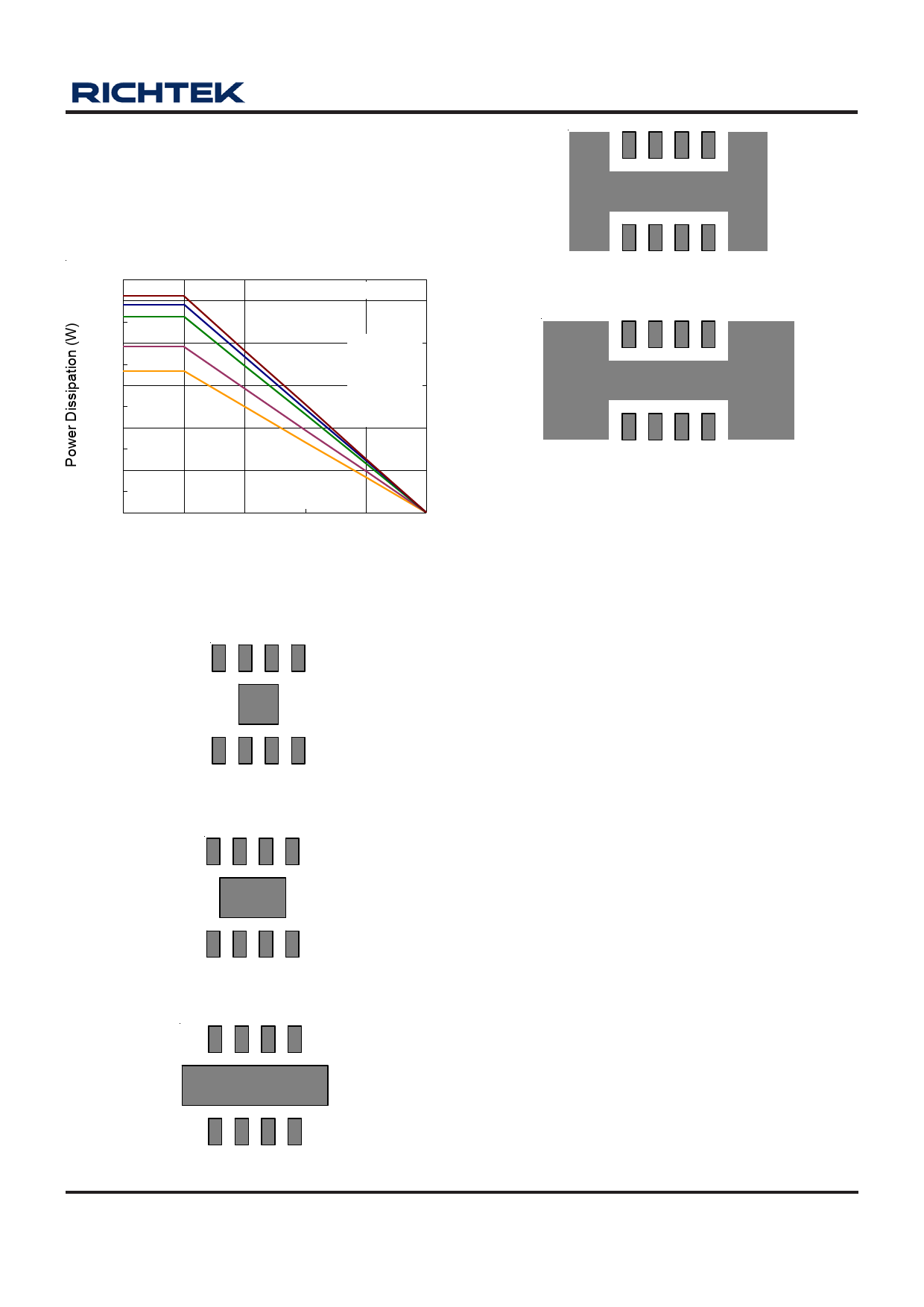
The maximum power dissipation depends on operating
ambient temperature for fixed TJ (MAX) and thermal
resistance θJA. For the RT8289, the Figure 5 of derating
curves allows the designer to see the effect of rising
ambient temperature on the maximum power dissipation
allowed.
2.2
Four Layer PCB
2.0
1.8
1.6
Copper Area
70mm2
1.4
50mm2
1.2
30mm2
1.0
10mm2
Min.Layout
0.8
0.6
0.4
0.2
0.0
0
25
50
75
100
125
Ambient Temperature (°C)
Figure 5. Derating Curves for RT8289 Package
(a) Copper Area = (2.3 x 2.3) mm2, θJA = 75°C/W
(b) Copper Area = 10mm2, θJA = 64°C/W
(d) Copper Area = 50mm2 , θJA = 51°C/W
(e) Copper Area = 70mm2 , θJA = 49°C/W
Figure 4. Themal Resistance vs. Copper Area Layout
Design
Layout Consideration
Follow the PCB layout guidelines for optimal performance
of the RT8289.
` Keep the traces of the main current paths as short and
wide as possible.
` Put the input capacitor as close as possible to the device
pins (VIN and GND).
` LX node is with high frequency voltage swing and should
be kept at small area. Keep analog components away
from the LX node to prevent stray capacitive noise pick-
up.
` Connect feedback network behind the output capacitors.
Keep the loop area small. Place the feedback
components near the RT8289.
` Connect all analog grounds to a command node and
then connect the command node to the power ground
behind the output capacitors.
` An example of PCB layout guide is shown in Figure 6 for
reference.
(c) Copper Area = 30mm2 , θJA = 54°C/W
DS8289-01 March 2011
www.richtek.com
11
Share Link: 